
Global Indium Phosphide Wafer Market Scope & Changing Dynamics 2025-2034
Global Indium Phosphide Wafer Market is segmented by Application (Photonics, 5G/Telecom, Data centers, Lidar, Defense optics), Type (Single-sided, Double-sided, Semi-insulating, Conductive, Ultra-thin), and Geography (North America, LATAM, West Europe, Central & Eastern Europe, Northern Europe, Southern Europe, East Asia, Southeast Asia, South Asia, Central Asia, Oceania, MEA)
Pricing
Report Overview
Industry Overview
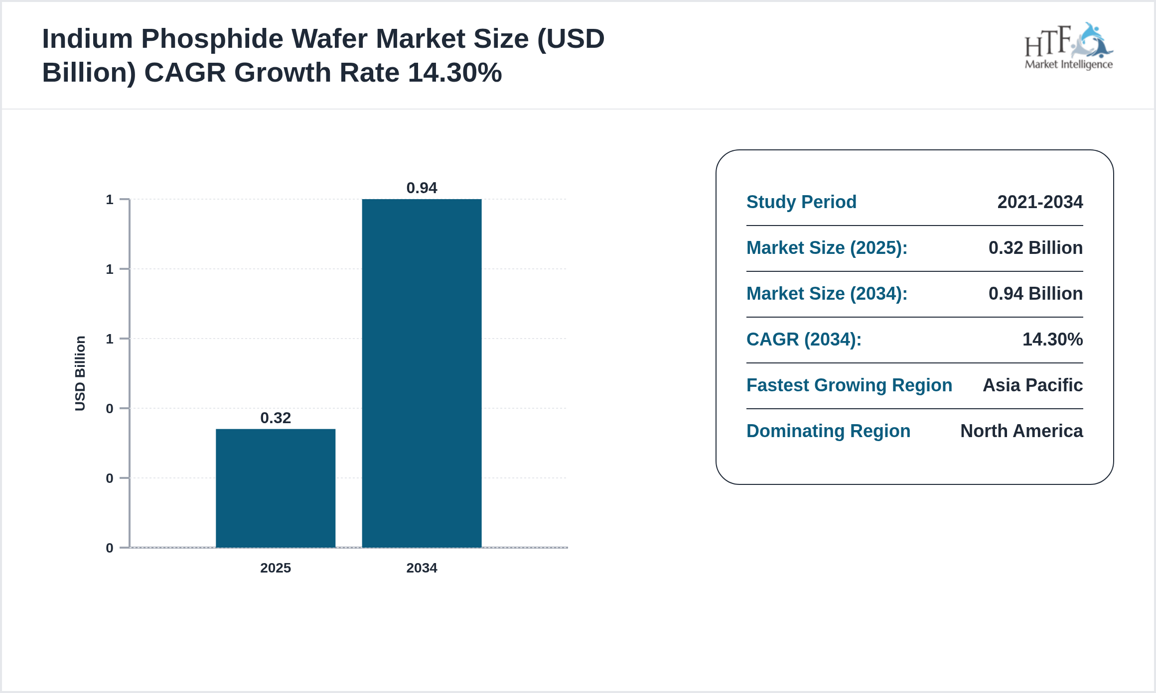
The Indium Phosphide Wafer market is witnessing significant growth and is expected to expand at a CAGR of 14.30% during the forecast period from 2025 to 2034. This growth is primarily driven by increasing technological advancements, rising consumer demand, and expanding applications across various industries. Businesses are increasingly adopting innovative solutions to improve operational efficiency, enhance customer experiences, and gain a competitive advantage, further fueling market expansion.
Source: HTF Market Intelligence (HTF MI)
The Global Indium Phosphide (InP) Wafer market includes semiconductor substrates used in high-speed optoelectronics, photonics, and high-frequency electronics. The ecosystem spans wafer manufacturers, epitaxy service providers, device fabricators, and end-user electronics companies. Scope covers InP wafers for lasers, photodetectors, transistors, and integrated circuits, while excluding silicon-based substrates. Market growth is driven by demand for 5G, data communication, defense electronics, and industrial automation. Supply chain integration involves precision crystal growth, quality testing, and logistics to semiconductor fabs. Commercial deployment models include direct wafer sales, supply agreements, and foundry partnerships. Sustainability initiatives focus on minimizing material waste, energy-efficient crystal growth, and recycling byproducts, supporting advanced manufacturing, high-performance device production, and revenue generation in the semiconductor industry
The research study Indium Phosphide Wafer Market gives readers information on tactical business choices and strategic planning that affect and stabilize the growth prediction in the Indium Phosphide Wafer market. However, a few disruptive trends will have opposite and significant effects on the distribution among players and the growth of the Indium Phosphide Wafer market. To give further advice on why certain developments in the Indium Phosphide Wafer market would have a significant impact and specifically why these trends can be taken into account when determining the market's trajectory and industry participants' strategic plans.
Key Highlights
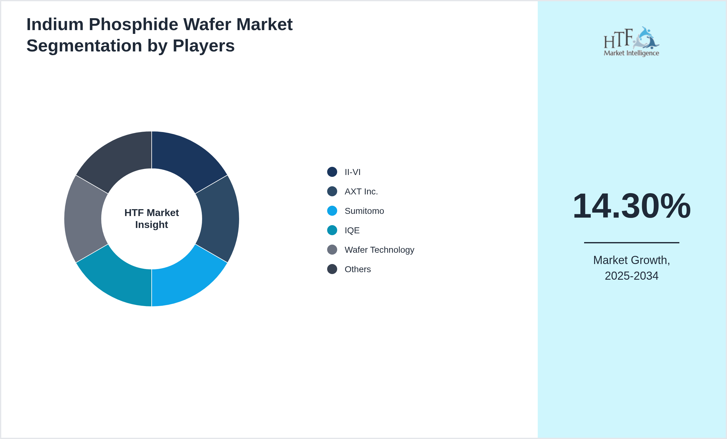
• The Indium Phosphide Wafer is growing at a CAGR of 14.30% during the forecasted period of 2025 to 2034
• Year-on-year growth for the market is 7.10%.
• North America dominated the market share in 2025
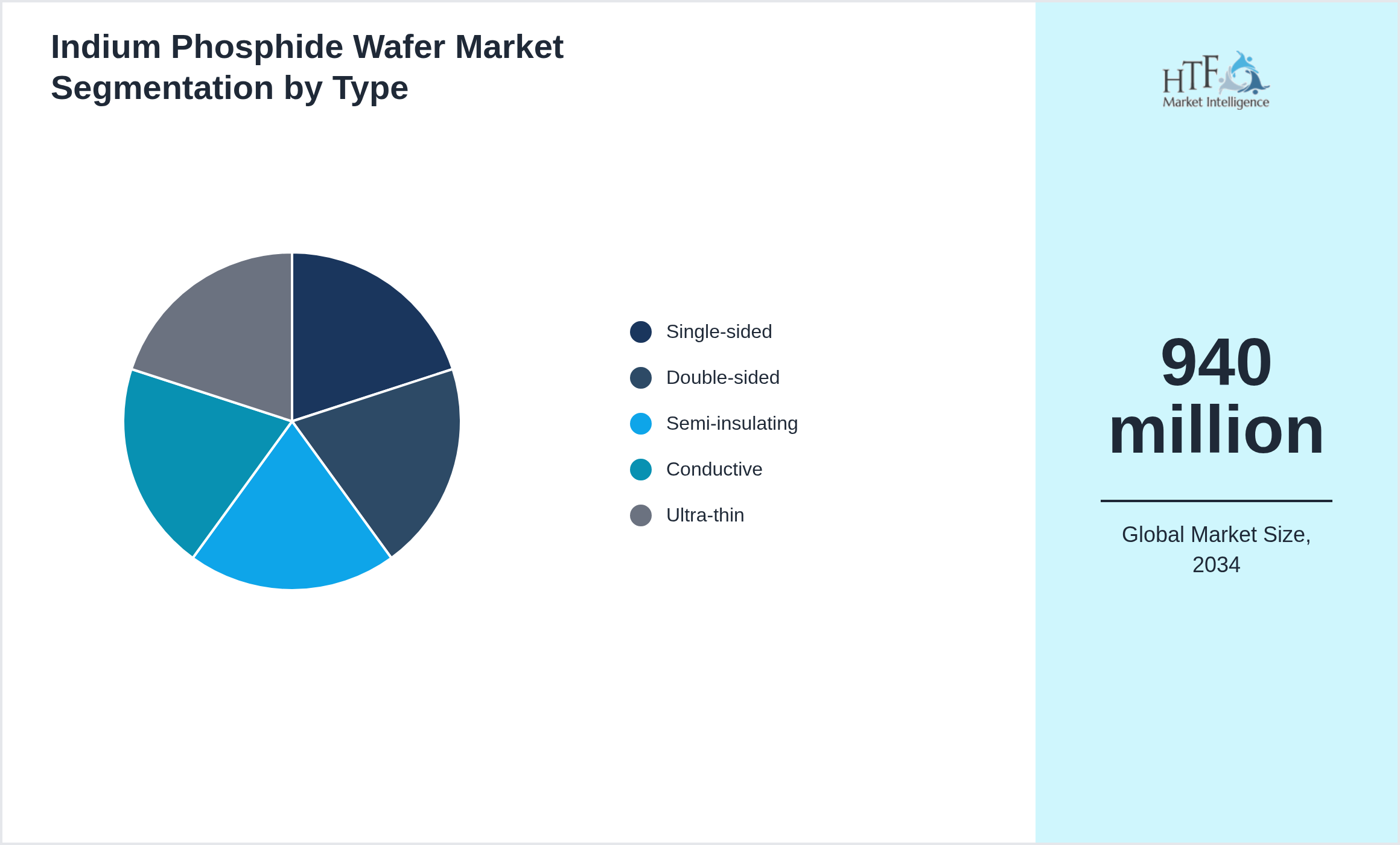
• Based on type, the market is bifurcated into the Single-sided, Double-sided, Semi-insulating, Conductive, Ultra-thin segment, which dominated the market share during the forecasted period
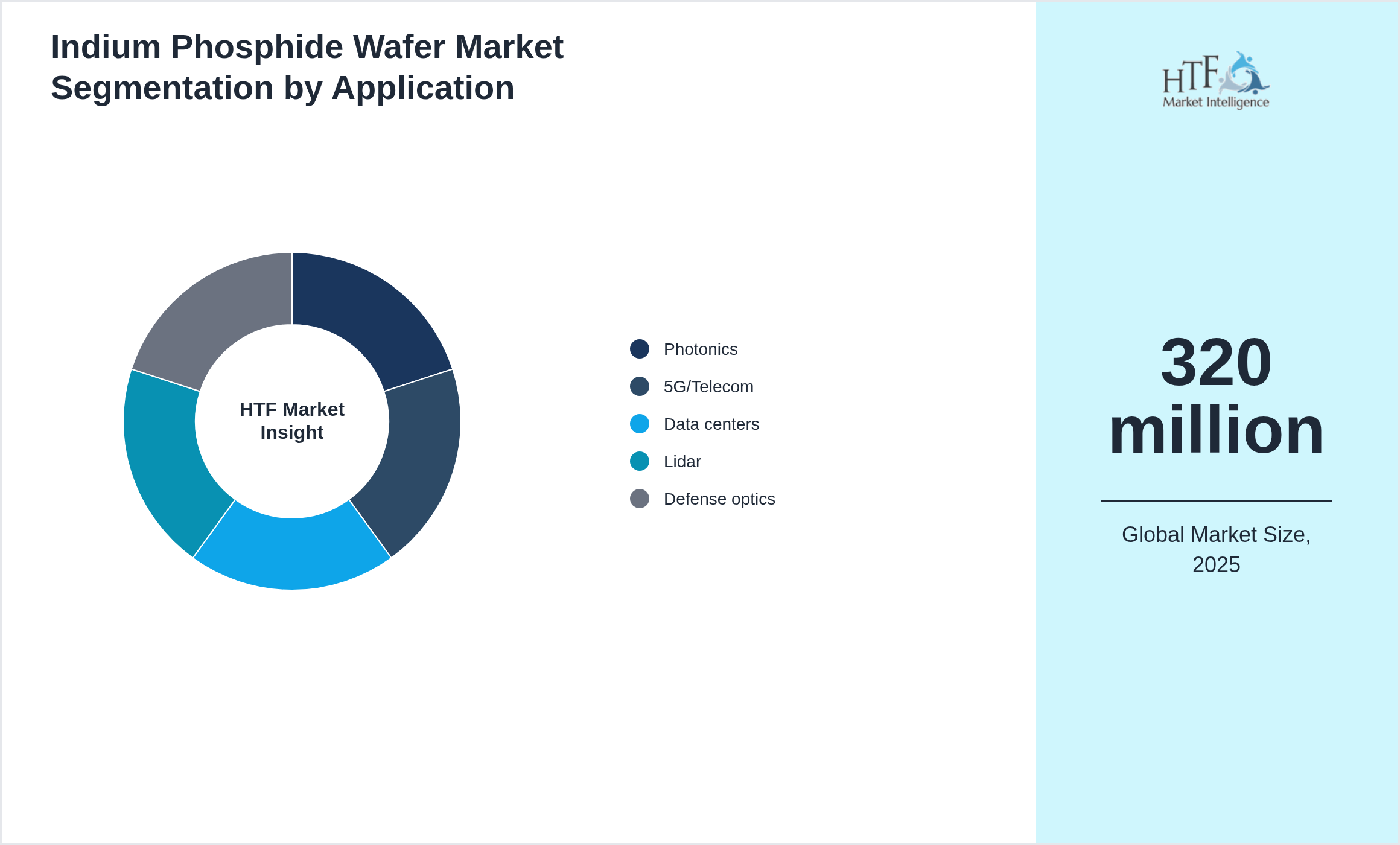
• Based on application, the market is segmented into Application Photonics, 5G/Telecom, Data centers, Lidar, Defense optics as the fastest-growing segment.
• North America, LATAM, West Europe, Central & Eastern Europe, Northern Europe, Southern Europe, East Asia, Southeast Asia, South Asia, Central Asia, Oceania, MEA import/export in terms of K tons, K units, and metric tons will be provided if applicable, based on industry best practices.
Market Dynamics Highlighted
Market Driver
The Indium Phosphide Wafer market is experiencing significant growth due to various factors.
- • The market is driven by increasing demand in high-speed electronics
Market Trend
The Indium Phosphide Wafer market is growing rapidly due to various factors.
- • Trends include epitaxial layer engineering
Opportunity
The Indium Phosphide Wafer has several opportunities, particularly in developing countries where industrialization is growing.
Challenge
The market for fluid power systems faces several obstacles despite its promising growth possibilities.
Indium Phosphide Wafer Market Segment Highlighted
Segmentation by Type
- • Single-sided
- • Double-sided
- • Semi-insulating
- • Conductive
- • Ultra-thin
Segmentation by Application
- • Photonics
- • 5G/Telecom
- • Data centers
- • Lidar
- • Defense optics
Key Players
The companies featured in this profile were selected based on insights from primary experts, evaluating their market penetration, product offerings, and geographical reach. By targeting emerging markets, these companies aim to leverage new opportunities, enhance their competitive advantage, and drive revenue growth. This approach not only aligns with their overall business objectives but also positions them to respond effectively to the evolving demands of consumers in these regions. Several key players in the Indium Phosphide Wafer market are strategically focusing on expanding their operations in developing regions to capture a larger market share, particularly as the year-on-year growth rate for the market stands at 7.10%.
- • II-VI
- • AXT Inc.
- • Sumitomo
- • IQE
- • Wafer Technology
- • GlobalWafers
- • Xiamen Powerway
- • Macom
- • InPhenix
- • CREE
- • Sivers Semiconductors
- • Broadcom
- • Nexxus Lighting
- • TQW
- • IntelliEpi
- • Finisar
- • Lumentum
- • NeoPhotonics
- • Skyworks
- • VPEC
Regional Insight
The North America dominant region currently dominates the market share, fueled by increasing consumption, population growth, and sustained economic progress, which collectively enhance market demand. Conversely, the Asia Pacific is growing rapidly, driven by significant infrastructure investments, industrial expansion, and rising consumer demand.
- North America
- LATAM
- West Europe
- Central & Eastern Europe
- Northern Europe
- Southern Europe
- East Asia
- Southeast Asia
- South Asia
- Central Asia
- Oceania
- MEA
- • North America: The US leads semiconductor and telecom applications with advanced manufacturing. Canada shows adoption in research and industrial electronics.
- • Europe: Germany UK and France dominate high-frequency semiconductor production and optoelectronics.
- • Asia-Pacific: China Japan South Korea and Taiwan expand adoption in telecom electronics and photonics industries.
- • Middle East & Africa: UAE and Saudi Arabia adopt for research and telecom applications. South Africa shows limited adoption.
- • Latin America: Brazil and Mexico gradually increase adoption in semiconductor manufacturing
Market Entropy
Merger & Acquisition
- • Feb 2024: IQE acquired InPTech Systems to expand indium phosphide wafer manufacturing globally targeting high-speed photonics and optoelectronic applications.
- • Aug 2024: Sumitomo Electric partnered with NanoWafer Labs to integrate high-purity epitaxial growth for telecom and data centers.
- • Mar 2025: WIN Semiconductors merged with AdvancedPhotonics Solutions to strengthen global supply chains for optical communication devices.
Patent Analysis
- • Dominates revenue due to high demand in photonics high-frequency electronics and optoelectronics; patented epitaxial growth polishing and doping processes enhance wafer quality and yield; automation in deposition and quality inspection reduces defect rates; shelf-life and stability technologies preserve wafer integrity during transport; supply-chain optimized for semiconductor fabrication plants; cost optimization via high-yield batch processes; end-user adoption driven by telecom aerospace and high-speed computing applications; premium pricing supported by material rarity and critical performance; contributes disproportionately to advanced semiconductor market revenue
Investment and Funding Scenario
- • Investment in indium phosphide wafers is growing via venture and private equity funding focused on high-purity semiconductor fabrication automated production and material innovation while partnerships with electronics and photonics manufacturers accelerate adoption infrastructure investments include fabrication plants R&D labs and analytical facilities trends indicate rising demand for high-speed optoelectronic and 5G applications recurring B2B supply contracts generate predictable revenue co-investments in process automation and quality control improve scalability and operational optimization strengthens market penetration profitability and long-term growth
Report Infographics
| Report Features | Details |
| Base Year | 2025 |
| Based Year Market Size (2025) | 320 million |
| Historical Period | 2021 to 2025 |
| CAGR (2025 to 2034) | 14.30% |
| Forecast Period | 2026 to 2034 |
| Forecasted Period Market Size (2034) | 940 million |
| Scope of the Report |
By Type, By Application, By Region |
| Companies Covered | II-VI, AXT Inc., Sumitomo, IQE, Wafer Technology, GlobalWafers, Xiamen Powerway, Macom, InPhenix, CREE, Sivers Semiconductors, Broadcom, Nexxus Lighting, TQW, IntelliEpi, Finisar, Lumentum, NeoPhotonics, Skyworks, VPEC |
| Customization Scope | 15% Free Customization
Want to Buy Specific Sections of This Report?
|
| Delivery Format | PDF and Excel through Email |
The Top-Down and Bottom-Up Approaches
The top-down approach begins with a broad theory or hypothesis and breaks it down into specific components for testing. This structured, deductive process involves developing a theory, creating hypotheses, collecting and analyzing data, and drawing conclusions. It is particularly useful when there is substantial theoretical knowledge, but it can be rigid and may overlook new phenomena.
Conversely, the bottom-up approach starts with specific data or observations, from which broader generalizations and theories are developed. This inductive process involves collecting detailed data, analyzing it for patterns, developing hypotheses, formulating theories, and validating them with additional data. While this approach is flexible and encourages the discovery of new phenomena, it can be time-consuming and less structured.
Regulatory Framework
The healthcare sector is overseen by various regulatory bodies that ensure the safety, quality, and efficacy of health services and products. In the United States, the U.S. Department of Health and Human Services (HHS) plays a crucial role in protecting public health and providing essential human services. Within HHS, the Food and Drug Administration (FDA) regulates food, drugs, and medical devices, ensuring they meet safety and efficacy standards. The Centers for Disease Control and Prevention (CDC) focuses on disease control and prevention, conducting research, and providing health information to protect public health.
Research enthusiast focused on transforming data uncovering into actionable insights through data-driven decision-making.