
United States 3D Ic And 2.5D Ic Packaging Market Scope & Changing Dynamics 2024-2034
United States 3D Ic And 2.5D Ic Packaging Market is segmented by Product Type (3D IC Packaging, 2.5D IC Packaging, Fan-Out Packaging, System in Package, Chip Scale Package), Application (Consumer Electronics, Automotive Electronics, Telecommunications, Healthcare Devices, Industrial Electronics), End-Use Industry (Consumer Electronics Manufacturing, Automotive Manufacturing, Telecommunications Services, Healthcare Equipment), Distribution Channel (Direct Sales, Distributors, Online Platforms), and Geography (Northeast, Southwest, The South, The Midwest)
Pricing
Report Overview
Executive Summary
- •The United States 3D IC and 2.5D IC Packaging market refers to the advanced semiconductor packaging technologies that vertically or horizontally integrate multiple integrated circuit dies to enhance performance, miniaturize devices, and improve electrical connectivity. 3D IC packaging stacks dies vertically through through-silicon vias (TSVs), while 2.5D IC packaging arranges dies side-by-side on an interposer substrate. These technologies are pivotal in enabling high-speed data transfer, increased power efficiency, and reduced device footprint. The market scope spans various packaging types, including fan-out wafer-level packaging and system-in-package solutions, targeting applications in consumer electronics, automotive, telecommunications, healthcare, and industrial electronics. The demand for more compact, high-performance chips in the United States drives innovation and adoption of these packaging technologies. Overall, this market is a critical segment of the semiconductor industry, supporting the development of next-generation electronic devices and the advancement of Internet of Things (IoT) ecosystems.
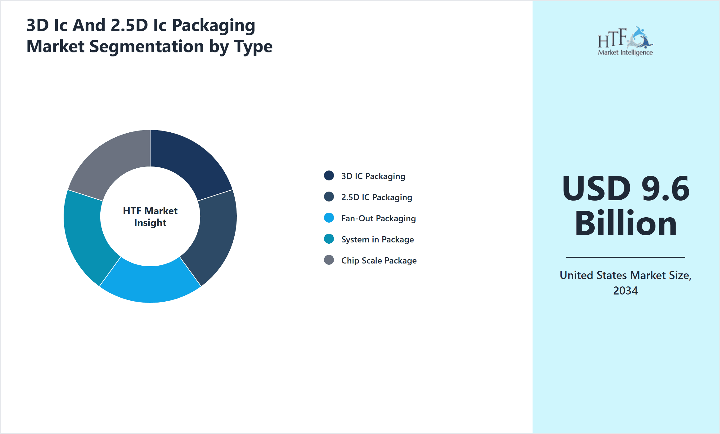
- •The United States market for 3D IC and 2.5D IC packaging is projected to grow from USD 3.2 billion in 2024 to USD 9.6 billion by 2034, reflecting a CAGR of approximately 11.6%. The growth is fueled by rising demand in consumer electronics and automotive sectors, alongside increasing investments in telecommunications infrastructure. Market dynamics indicate a strong shift toward fan-out packaging techniques and system-in-package solutions, which offer enhanced integration capabilities. The West Coast region dominates the market due to the presence of leading semiconductor companies and R&D centers, while the Southeast region is the fastest growing, driven by expanding manufacturing hubs.
- •The 3D IC and 2.5D IC packaging market holds strategic importance for industries requiring high computing power and miniaturized form factors, including smartphones, automotive electronics, and healthcare devices. For stakeholders such as semiconductor manufacturers, device OEMs, and packaging service providers, the market offers opportunities to leverage innovations in packaging technologies to meet stringent performance and thermal management requirements. The market's evolution is integral to sustaining the United States' leadership in semiconductor technology and addressing increasing global competition. Enhanced packaging solutions enable faster time-to-market and improved product differentiation, making the sector a critical focus area for R&D and investment.

Competitive Landscape
The competitive landscape of the United States 3D IC and 2.5D IC Packaging market is characterized by intense rivalry among leading semiconductor packaging companies, technology innovators, and foundries. Market players focus on differentiating through technological advancements such as improved thermal dissipation, higher interconnect density, and miniaturization capabilities. Strategic partnerships and collaborations with chip designers and OEMs are common to accelerate product development and integration. Innovation is driven by heavy R&D investments aimed at developing next-generation packaging solutions that address challenges of power efficiency and signal integrity. Competitive strategies also include mergers and acquisitions to consolidate market position and expand technology portfolios. Regional hubs like the West Coast benefit from dense networks of semiconductor expertise, providing companies with competitive advantages in agility and innovation. Pricing strategies and supply chain optimization remain critical factors in maintaining market leadership amid evolving customer demands.
Leading Companies in 3D Ic And 2.5D Ic Packaging Market
- •Intel Corporation (United States)
- •Amkor Technology, Inc. (United States)
- •Texas Instruments Incorporated (United States)
- •Analog Devices, Inc. (United States)
- •Broadcom Inc. (United States)
- •Skyworks Solutions, Inc. (United States)
- •Advanced Micro Devices, Inc. (United States)
- •NVIDIA Corporation (United States)
- •Microchip Technology Inc. (United States)
- •ON Semiconductor Corporation (United States)
- •Qorvo, Inc. (United States)
- •Maxim Integrated (United States)
- •Analogic Corporation (United States)
- •Lattice Semiconductor Corporation (United States)
- •SkyWater Technology Foundry (United States)
- •Cadence Design Systems, Inc. (United States)
- •Micron Technology, Inc. (United States)
- •Xilinx, Inc. (United States)
- •Synaptics Incorporated (United States)
- •Marvell Technology Group Ltd. (United States)
- •Cirrus Logic, Inc. (United States)
- •Cree, Inc. (United States)
- •ON Semiconductor (United States)
- •TE Connectivity Ltd. (United States)
- •NXP Semiconductors N.V. (United States)

Market Breakdown
- •By Product Type
- ◦3D IC Packaging
- ◦2.5D IC Packaging
- ◦Fan-Out Packaging
- ◦System in Package
- ◦Chip Scale Package
- •By Application
- ◦Consumer Electronics
- ◦Automotive Electronics
- ◦Telecommunications
- ◦Healthcare Devices
- ◦Industrial Electronics
- •By End-Use Industry
- ◦Consumer Electronics Manufacturing
- ◦Automotive Manufacturing
- ◦Telecommunications Services
- ◦Healthcare Equipment
- •By Distribution Channel
- ◦Direct Sales
- ◦Distributors
- ◦Online Platforms
Growth Dynamics
- •Rising demand for compact and high-performance electronic devices in the United States is driving increased adoption of 3D and 2.5D IC packaging technologies. These packaging methods enable greater integration density, improving speed and power efficiency in consumer and automotive electronics.
- •Technological advancements such as fan-out wafer-level packaging and system-in-package solutions are enhancing the functional capabilities and thermal management of semiconductor devices, fueling market growth and expanding the addressable application areas.
- •Government initiatives supporting semiconductor manufacturing and innovation, including incentives for domestic production, are contributing to capacity expansions and investments in advanced packaging facilities across key U.S. regions.
- •The proliferation of 5G networks and IoT devices is creating increased demand for high-speed, low-latency packaging solutions, positioning 3D and 2.5D IC technologies as essential enablers for telecommunications and industrial electronics sectors.
- •Strategic collaborations between semiconductor foundries, packaging service providers, and chipset manufacturers are accelerating innovation cycles and improving product adoption rates in the highly competitive U.S. market.
Market Trends
- •The market is witnessing a trend toward fan-out packaging techniques, which provide thinner package profiles and improved thermal performance, increasingly preferred over traditional 3D stacking for certain applications.
- •Integration of heterogeneous materials and chips in system-in-package formats is gaining traction, enabling multifunctional devices that combine logic, memory, and sensors in compact form factors.
- •Increased focus on sustainability and eco-friendly materials in packaging processes is influencing R&D priorities, with companies aiming to reduce environmental impact without compromising performance.
- •Emerging adoption of AI-driven design tools is optimizing packaging layouts and thermal management, accelerating time-to-market for complex semiconductor packages.
- •Regional supply chain diversification efforts are reshaping manufacturing footprints, with increased investments outside traditional hubs to mitigate risks and meet rising domestic demand.

Market Opportunities
- •Expanding automotive electronics demand for advanced driver-assistance systems (ADAS) and electric vehicle powertrains presents significant growth potential for 3D and 2.5D IC packaging solutions customized for harsh environments.
- •Emerging healthcare applications requiring miniaturized, high-performance devices offer opportunities for packaging innovations that improve signal integrity and integration density.
- •Investment in domestic packaging infrastructure backed by federal incentives enables companies to scale production capabilities and reduce reliance on overseas suppliers.
- •Development of next-generation interconnect materials and TSV technologies can unlock higher performance thresholds and open new application segments in AI and high-performance computing.
- •Strategic partnerships with chip designers and OEMs to co-develop customized packaging solutions can create strong competitive differentiation and customer loyalty.
Market Challenges
- •High manufacturing complexity and costs associated with 3D IC and 2.5D IC packaging limit widespread adoption, especially for cost-sensitive consumer electronics segments.
- •Technical challenges related to thermal management and reliability of vertically stacked dies require continuous innovation and rigorous testing protocols, impacting time-to-market.
- •Shortage of skilled workforce specialized in advanced packaging techniques poses a bottleneck for capacity expansions and innovation in the United States.
- •Stringent regulatory and environmental compliance requirements increase operational costs and complexity of packaging manufacturing processes.
- •Intense competition from Asian packaging service providers offering cost advantages challenges U.S.-based manufacturers to maintain market share.
Regulatory Framework
Between 2020 and 2024, the United States government implemented the CHIPS Act, providing significant subsidies and incentives aimed at strengthening domestic semiconductor manufacturing, including advanced packaging facilities. Compliance with environmental and safety standards under the Environmental Protection Agency (EPA) has been enforced to reduce the ecological impact of semiconductor production. Additionally, the Federal Communications Commission (FCC) mandates adherence to electromagnetic compatibility and radio frequency standards, critical for packaging in telecommunications applications. The Occupational Safety and Health Administration (OSHA) updated guidelines to address worker safety in high-tech manufacturing environments, emphasizing chemical handling and cleanroom protocols. This regulatory environment fosters innovation while ensuring sustainable and safe operational practices across the 3D IC and 2.5D IC packaging ecosystem in the United States.
Market Intelligence
- •15th January 2025, Intel Corporation announced the launch of a new 3D IC packaging technology featuring improved thermal management and increased interconnect density tailored for next-generation AI processors. This innovation is expected to reduce power consumption by 20% while enhancing data transfer speeds, targeting high-performance computing and data center applications. The technology integrates advanced through-silicon vias with fan-out wafer-level packaging, marking a significant leap in the semiconductor packaging landscape. Intel’s strategic objective is to solidify its leadership in the advanced packaging segment within the United States and globally, responding to growing market demand for compact, efficient chip designs. Source: Intel Official Press Release
- •20th March 2025, Amkor Technology, Inc. introduced a novel 2.5D IC packaging platform designed for automotive electronics, emphasizing superior thermal dissipation and mechanical robustness. The platform supports heterogeneous integration of logic and memory chips, enhancing system reliability in harsh automotive environments. Amkor’s innovation aims to address the rising complexity of automotive semiconductor requirements driven by electric vehicles and autonomous driving technologies. This development strengthens Amkor’s portfolio and aligns with increasing domestic demand for advanced packaging solutions in the automotive sector. Source: Amkor Technology Corporate Announcement
- •10th February 2025, Texas Instruments Incorporated announced a strategic partnership with a leading foundry to co-develop system-in-package solutions optimized for 5G telecommunications infrastructure. The collaboration focuses on enhancing signal integrity and reducing package size to support dense antenna arrays and edge computing devices. This partnership is expected to accelerate deployment timelines for 5G base stations across the United States, responding to the expanding telecom market. Texas Instruments aims to leverage this alliance to boost its market share in advanced packaging for communications. Source: Texas Instruments Press Release
- •5th April 2025, Analog Devices, Inc. completed the acquisition of a U.S.-based fan-out packaging startup, enhancing its capabilities in wafer-level packaging technology. The acquisition is part of Analog Devices’ strategy to expand its product offerings in high-density, high-performance packaging solutions targeting industrial and healthcare electronics. This move consolidates Analog’s position in the competitive U.S. market and accelerates innovation cycles for miniaturized device applications. The integration of the startup’s technology is expected to generate synergies in R&D and manufacturing. Source: Analog Devices Corporate News
Regional Outlook
The West Coast currently holds a significant share of the market, primarily due to several key factors: increasing consumption rates, a burgeoning population, and robust economic momentum. These elements collectively drive demand, positioning this region as a leader in the market. On the other hand, Southeast is rapidly emerging as the fastest-growing area within the industry. This remarkable growth can be attributed to swift infrastructure development, the expansion of various industrial sectors, and a marked increase in consumer demand. These dynamics make this region a crucial player in shaping future market growth.
In our report, we cover a comprehensive analysis of the following regions and countries:
- Northeast
- Southwest
- The South
- The Midwest
| Feature | Details |
|---|---|
| Base Year Market Size | USD 3.2 Billion |
| Forecast Year Market Size | USD 9.6 Billion |
| CAGR | 11.61% |
| Forecast Period | 2026 to 2033 |
| YoY Growth | 11.04% |
| Scope of Report | Market is segmented by Product Type (3D IC Packaging, 2.5D IC Packaging, Fan-Out Packaging, System in Package, Chip Scale Package), Application (Consumer Electronics, Automotive Electronics, Telecommunications, Healthcare Devices, Industrial Electronics), End-Use Industry (Consumer Electronics Manufacturing, Automotive Manufacturing, Telecommunications Services, Healthcare Equipment), Distribution Channel (Direct Sales, Distributors, Online Platforms) |
| Regions Covered | Northeast, Southwest, The South, The Midwest |
| Key Companies | Intel Corporation (United States), Amkor Technology, Inc. (United States), Texas Instruments Incorporated (United States), Analog Devices, Inc. (United States), Broadcom Inc. (United States), Skyworks Solutions, Inc. (United States), Advanced Micro Devices, Inc. (United States), NVIDIA Corporation (United States), Microchip Technology Inc. (United States), ON Semiconductor Corporation (United States), Qorvo, Inc. (United States), Maxim Integrated (United States), Analogic Corporation (United States), Lattice Semiconductor Corporation (United States), SkyWater Technology Foundry (United States), Cadence Design Systems, Inc. (United States), Micron Technology, Inc. (United States), Xilinx, Inc. (United States), Synaptics Incorporated (United States), Marvell Technology Group Ltd. (United States), Cirrus Logic, Inc. (United States), Cree, Inc. (United States), ON Semiconductor (United States), TE Connectivity Ltd. (United States), NXP Semiconductors N.V. (United States) |
United States 3D Ic And 2.5D Ic Packaging Market Scope & Changing Dynamics 2024-2034 - Table of Contents
Frequently Asked Questions (FAQ):
The Compact Track Loaders market is projected to grow at a CAGR of 6.8% from 2025 to 2030, driven by increasing demand in construction and agricultural sectors.
North America currently leads the market with approximately 45% market share, followed by Europe at 28% and Asia-Pacific at 22%. The remaining regions account for 5% of the global market.
Key growth drivers include increasing construction activities, rising demand for versatile equipment in agriculture, technological advancements in track loader design, and growing preference for compact equipment in urban construction projects.