
Asia-Pacific Ceramic Dummy Wafer Market Size, Growth & Revenue 2025-2034
Asia-Pacific Ceramic Dummy Wafer Market is segmented by Type (Single-Side Polished Ceramic Dummy Wafers, Double-Side Polished Ceramic Dummy Wafers, Fully Polished Ceramic Dummy Wafers, Patterned Ceramic Dummy Wafers, Standard Ceramic Dummy Wafers), Application (Semiconductor Fabrication, Wafer Testing, Equipment Calibration, Process Optimization, Research & Development), Wafer Diameter (150 mm, 200 mm, 300 mm, 450 mm), Material Grade (High Purity Ceramic, Standard Purity Ceramic, Customized Ceramic Grades), and Geography (Japan, China, Southeast Asia, India, Australia, South Korea, Others)
Pricing
Report Overview
Executive Summary
- •The Asia-Pacific Ceramic Dummy Wafer market encompasses the production and utilization of non-functional semiconductor wafers designed to simulate real wafers in fabrication and testing processes. These ceramic wafers play a vital role in semiconductor manufacturing by enabling precise equipment calibration, process tuning, and contamination control without risking valuable silicon wafers. The market scope includes various wafer types such as single-side polished, double-side polished, fully polished, patterned, and standard dummy wafers, serving applications in semiconductor fabrication, wafer testing, equipment calibration, process optimization, and research and development. The increasing semiconductor production capacity in Asia-Pacific, fueled by investments in advanced fabrication plants and rising demand for electronic devices, amplifies the need for high-quality ceramic dummy wafers. The market integrates cutting-edge manufacturing technologies and material innovations to meet stringent wafer standards, contributing to improved yield and reduced downtime in semiconductor fabs. This market's significance is heightened by the region’s strategic positioning as a global semiconductor manufacturing hub and the continuous evolution of semiconductor devices requiring precise process control and testing infrastructure.
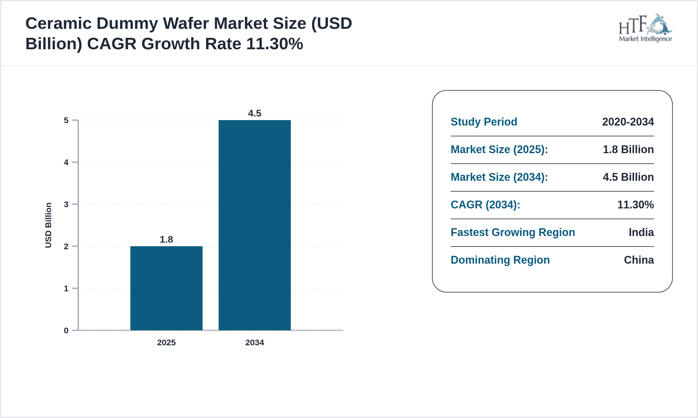
- •Key highlights include a robust compound annual growth rate of 11.3% projected from 2025 to 2034, with the market size expected to expand from USD 1.8 billion in 2025 to approximately USD 4.5 billion by 2034. China dominates the market due to its extensive semiconductor manufacturing infrastructure, while India exhibits the fastest growth driven by government initiatives fostering semiconductor fabrication capabilities. Double-side polished ceramic dummy wafers hold the largest market share attributable to their superior surface quality and applicability in advanced process nodes. Patterned dummy wafers are experiencing rapid adoption as device architectures become more complex, demanding more precise calibration and testing solutions. The semiconductor fabrication application segment leads due to the increasing integration of dummy wafers in contamination control and process optimization workflows.
- •The Asia-Pacific Ceramic Dummy Wafer market presents strategic value to semiconductor manufacturers, equipment suppliers, and materials providers by enabling enhanced process reliability and manufacturing efficiency. Stakeholders benefit from adopting advanced dummy wafer technologies to reduce process variability and improve tool uptime, directly impacting production yields and cost-effectiveness. The market supports the region’s semiconductor ecosystem growth by aligning with initiatives such as China’s ‘Made in China 2025’ and India’s ‘Semiconductor Mission,’ which prioritize domestic manufacturing capabilities. The expanding consumer electronics, automotive semiconductor, and industrial electronics sectors further underscore the importance of ceramic dummy wafers in sustaining the region’s semiconductor competitiveness. Collaborative innovation, regulatory compliance, and investments in wafer fabrication capabilities define the market’s strategic trajectory in the Asia-Pacific landscape.
Competitive Landscape
The Asia-Pacific Ceramic Dummy Wafer market operates within a highly competitive environment where companies leverage strategic partnerships, continuous product innovation, and geographical expansion to strengthen market presence. Leading players focus on advancing polishing technologies and wafer patterning techniques to meet increasingly stringent semiconductor manufacturing requirements. Adoption of automation and precision manufacturing processes enhances product quality and operational efficiency. Firms engage in collaborative development agreements with semiconductor fabs and equipment manufacturers to tailor dummy wafer solutions that optimize equipment calibration and process control. Regional expansion into emerging markets such as India and Southeast Asia enables access to burgeoning semiconductor fabrication investments. Companies differentiate themselves through comprehensive product portfolios, stringent quality standards, and responsiveness to evolving semiconductor node complexities. The integration of sustainable manufacturing practices and compliance with environmental regulations further positions companies to capture growing market segments. Strategic mergers and acquisitions consolidate market share while facilitating technology transfer and innovation acceleration. The competitive landscape remains dynamic, driven by technological advancements, evolving customer requirements, and the rapid expansion of semiconductor manufacturing capacity within Asia-Pacific.
Prominent Players in Ceramic Dummy Wafer Market
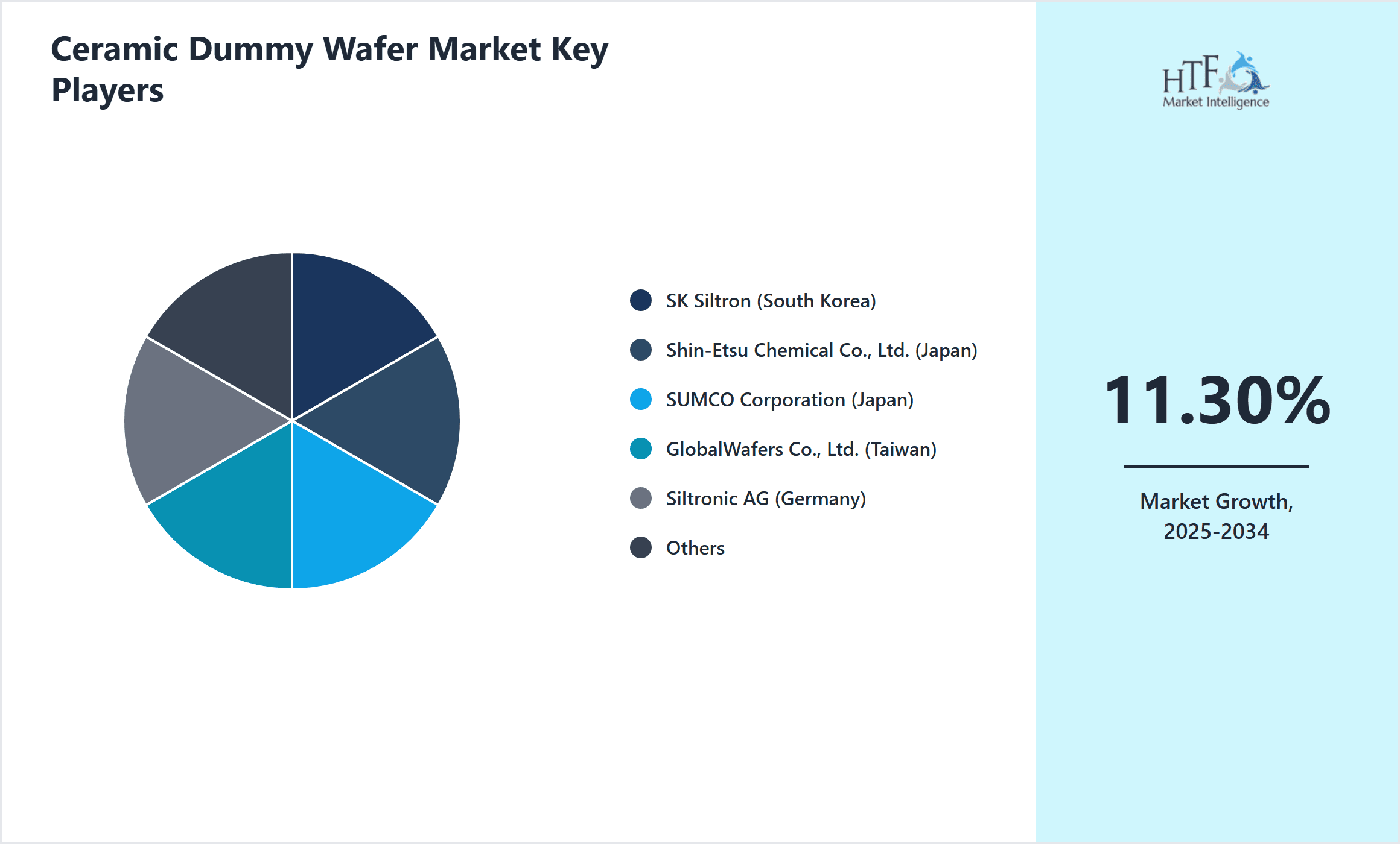
- •SK Siltron (South Korea)
- •Shin-Etsu Chemical Co., Ltd. (Japan)
- •SUMCO Corporation (Japan)
- •GlobalWafers Co., Ltd. (Taiwan)
- •Siltronic AG (Germany)
- •MEMC Electronic Materials (United States)
- •Silicon Works (South Korea)
- •Wafer Works Corporation (Taiwan)
- •Shandong Crystal Silicon Electronics Technology Co., Ltd. (China)
- •LG Siltron (South Korea)
- •Nippon Steel Corporation (Japan)
- •Dowa Electronics Materials Co., Ltd. (Japan)
- •Advanced Semiconductor Materials America, Inc. (United States)
- •Silicon Valley Microelectronics, Inc. (Taiwan)
- •China Wafer Technology Co., Ltd. (China)
- •Topsil Semiconductor Materials A/S (Denmark)
- •Tokuyama Corporation (Japan)
- •Global Advanced Materials Group (Singapore)
- •SEMICORE Corporation (South Korea)
- •Central Semiconductor Corporation (United States)
Market Breakdown
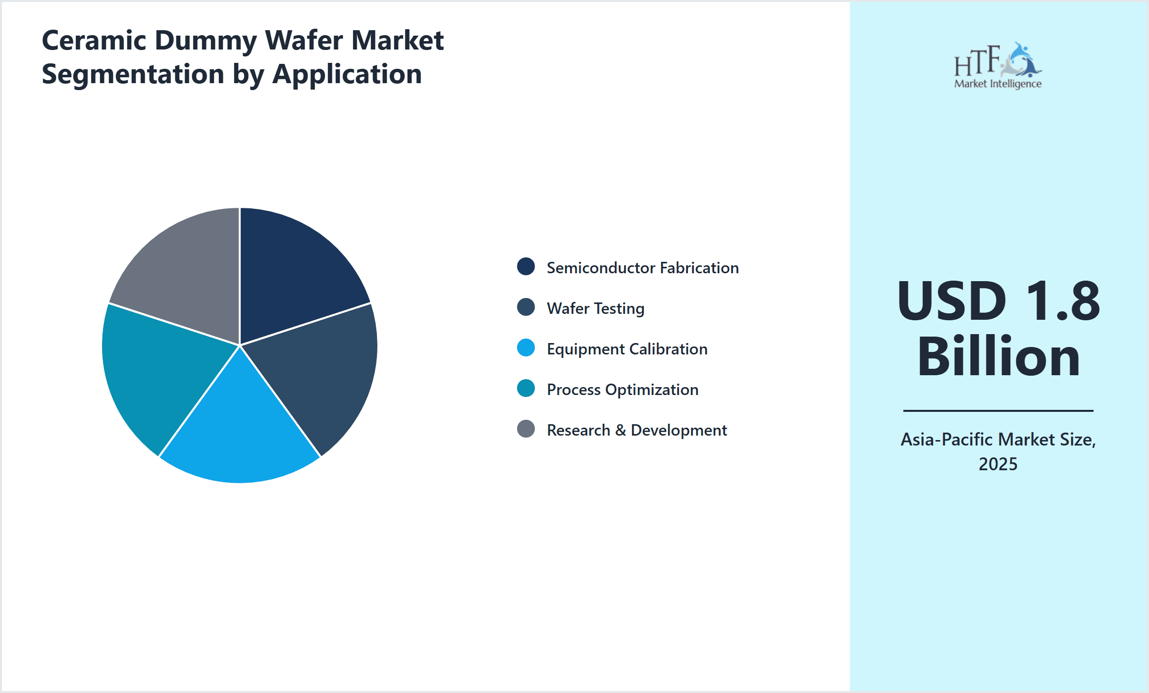
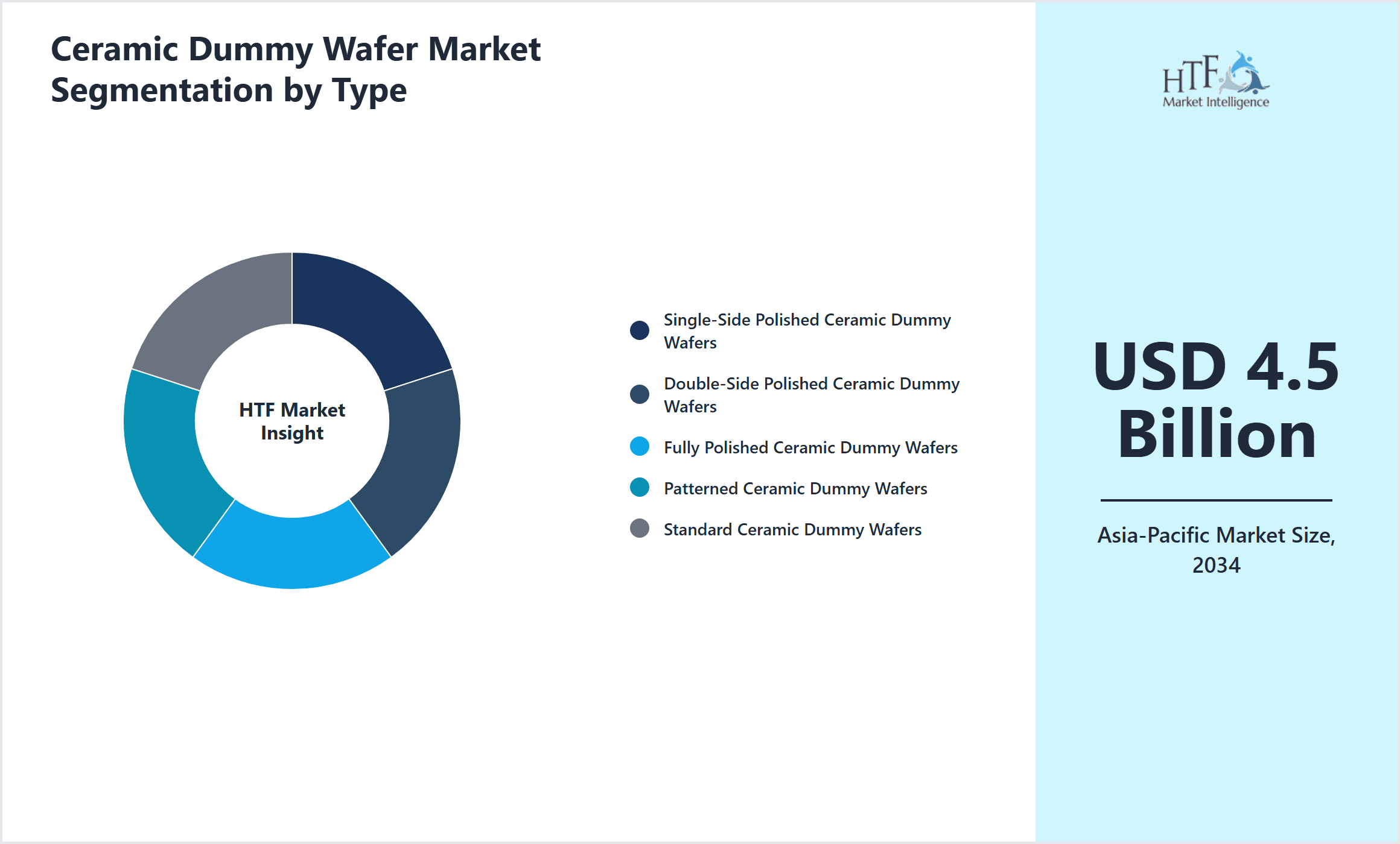
- •By Type
- ◦Single-Side Polished Ceramic Dummy Wafers
- ◦Double-Side Polished Ceramic Dummy Wafers
- ◦Fully Polished Ceramic Dummy Wafers
- ◦Patterned Ceramic Dummy Wafers
- ◦Standard Ceramic Dummy Wafers
- •By Application
- ◦Semiconductor Fabrication
- ◦Wafer Testing
- ◦Equipment Calibration
- ◦Process Optimization
- ◦Research & Development
- •By Wafer Diameter
- ◦150 mm
- ◦200 mm
- ◦300 mm
- ◦450 mm
- •By Material Grade
- ◦High Purity Ceramic
- ◦Standard Purity Ceramic
- ◦Customized Ceramic Grades
Growth Dynamics
Rising semiconductor manufacturing activities across Asia-Pacific drive significant demand for ceramic dummy wafers, as fabs require precise calibration tools to maintain process accuracy. Increasing adoption of advanced nodes in semiconductor fabrication escalates the need for high-grade dummy wafers to simulate physical and thermal characteristics accurately, ensuring equipment performance and yield consistency. Government initiatives such as China’s 'Made in China 2025' and India’s 'Semiconductor Mission' emphasize domestic semiconductor production expansion, directly boosting ceramic dummy wafer consumption. Manufacturers integrate innovative polishing and patterning technologies to meet evolving wafer specifications, enhancing overall production efficiency and reducing downtime. The proliferation of consumer electronics, automotive semiconductors, and industrial IoT devices further intensifies the need for reliable dummy wafers to support complex fabrication processes. Recent collaborations between material suppliers and semiconductor fabs underscore strategic efforts to develop specialized ceramic dummy wafers tailored to emerging fabrication challenges, reinforcing market growth momentum.
Market Trends
Emerging trends in the Asia-Pacific Ceramic Dummy Wafer market include increasing utilization of patterned ceramic dummy wafers that replicate complex device architectures, enabling more accurate equipment calibration and process control in advanced semiconductor nodes. Integration of automation and AI-driven quality inspection systems in dummy wafer manufacturing enhances precision and reduces defect rates. Growing emphasis on sustainability drives adoption of eco-friendly ceramic materials and energy-efficient manufacturing processes. Expansion of 300 mm and 450 mm wafer diameter dummy wafers aligns with industry trends towards larger wafer formats to improve production throughput. Strategic expansion of manufacturing facilities in India and Southeast Asia aims to capture rising local semiconductor fabrication investments. Collaboration between dummy wafer producers and semiconductor equipment manufacturers fosters co-development of wafer solutions optimized for next-generation semiconductor technologies. Digital twin and simulation technologies increasingly complement physical dummy wafer usage, allowing foresight in process adjustments and equipment calibration enhancement.
Market Opportunities
Significant opportunities arise from the rapid expansion of semiconductor fabs in India and Southeast Asia, creating new demand pockets for ceramic dummy wafers tailored to regional manufacturing needs. Technological advances in ceramic material science offer opportunities to develop higher purity and mechanically robust dummy wafers, improving equipment calibration accuracy and longevity. The rise of 5G, AI, and automotive electronics accelerates demand for advanced semiconductor devices, indirectly boosting the ceramic dummy wafer market. Collaborative innovation between material suppliers and semiconductor fabs enables customized dummy wafer solutions addressing unique process challenges. Opportunities also emerge from increasing adoption of larger wafer diameters, requiring new dummy wafer designs and fabrication capabilities. Strategic partnerships with semiconductor equipment manufacturers facilitate integrated calibration solutions, expanding market reach. Expansion into R&D applications supports early-stage device development, providing diversified revenue streams. Government subsidies and incentives in Asia-Pacific countries stimulate investments in semiconductor infrastructure, fostering sustained dummy wafer market growth.
Market Challenges
High precision and quality requirements for ceramic dummy wafers present significant manufacturing challenges, as deviations can adversely affect semiconductor fab tool calibration and yield. Supply chain disruptions impacting the availability of high-purity ceramic materials hamper production schedules and increase costs. Intense competition from silicon and other material-based dummy wafers imposes pricing pressures on ceramic wafer manufacturers. The need for continuous technological upgrades to match evolving semiconductor nodes demands substantial R&D investments, which may burden smaller players. Regulatory complexities related to material handling and environmental compliance add operational constraints. Recent geopolitical tensions impacting raw material imports have caused delays for some Asia-Pacific manufacturers. Additionally, the lack of standardized dummy wafer specifications across fabs complicates product development and customer adaptation. These factors collectively pose barriers to market entry and expansion, requiring sustained innovation and strategic agility from industry participants.
Regulatory Framework
The Asia-Pacific Ceramic Dummy Wafer market operates under stringent regulatory frameworks focusing on environmental safety, material purity, and workplace handling standards. In China, the 2019 Environmental Protection Law amendments mandated stricter emissions control and waste management protocols for ceramic material manufacturing, compelling producers to adopt cleaner technologies. India’s 2022 Semiconductor Policy includes guidelines promoting eco-friendly manufacturing processes and incentivizing compliance with chemical handling standards to reduce environmental impact. Japan enforces the Chemical Substances Control Law updates introduced in 2021, emphasizing material safety and hazardous substance management in wafer production. South Korea’s Ministry of Environment regulations updated in 2023 require transparent reporting of material sourcing and adherence to sustainable manufacturing certifications. These regulations collectively ensure that ceramic dummy wafer producers maintain high standards in product quality, environmental stewardship, and occupational safety, supporting sustainable industry growth across Asia-Pacific.
Market Intelligence
Recent market developments and strategic initiatives are continuously tracked through industry publications, company announcements, and regulatory filings. For the most current information, stakeholders are advised to monitor official corporate communications and recognized market intelligence platforms.
Regional Outlook
The China currently holds a significant share of the market, primarily due to several key factors: increasing consumption rates, a burgeoning population, and robust economic momentum. These elements collectively drive demand, positioning this region as a leader in the market. On the other hand, India is rapidly emerging as the fastest-growing area within the industry. This remarkable growth can be attributed to swift infrastructure development, the expansion of various industrial sectors, and a marked increase in consumer demand. These dynamics make this region a crucial player in shaping future market growth.
In our report, we cover a comprehensive analysis of the following regions and countries:
- Japan
- China
- Southeast Asia
- India
- Australia
- South Korea
- Others
| Feature | Details |
|---|---|
| Base Year Market Size | USD 1.8 Billion |
| Forecast Year Market Size | USD 4.5 Billion |
| CAGR | 11.3% |
| Forecast Period | 2026 to 2033 |
| YoY Growth | 11.3% |
| Scope of Report | Market is segmented by Type (Single-Side Polished Ceramic Dummy Wafers, Double-Side Polished Ceramic Dummy Wafers, Fully Polished Ceramic Dummy Wafers, Patterned Ceramic Dummy Wafers, Standard Ceramic Dummy Wafers), Application (Semiconductor Fabrication, Wafer Testing, Equipment Calibration, Process Optimization, Research & Development), Wafer Diameter (150 mm, 200 mm, 300 mm, 450 mm), Material Grade (High Purity Ceramic, Standard Purity Ceramic, Customized Ceramic Grades) |
| Regions Covered | Japan, China, Southeast Asia, India, Australia, South Korea, Others |
| Key Companies | SK Siltron (South Korea), Shin-Etsu Chemical Co., Ltd. (Japan), SUMCO Corporation (Japan), GlobalWafers Co., Ltd. (Taiwan), Siltronic AG (Germany), MEMC Electronic Materials (United States), Silicon Works (South Korea), Wafer Works Corporation (Taiwan), Shandong Crystal Silicon Electronics Technology Co., Ltd. (China), LG Siltron (South Korea), Nippon Steel Corporation (Japan), Dowa Electronics Materials Co., Ltd. (Japan), Advanced Semiconductor Materials America, Inc. (United States), Silicon Valley Microelectronics, Inc. (Taiwan), China Wafer Technology Co., Ltd. (China), Topsil Semiconductor Materials A/S (Denmark), Tokuyama Corporation (Japan), Global Advanced Materials Group (Singapore), SEMICORE Corporation (South Korea), Central Semiconductor Corporation (United States) |
Asia-Pacific Ceramic Dummy Wafer Market Size, Growth & Revenue 2025-2034 - Table of Contents
Multidisciplinary researcher with 10+ years of experience uncovering insights across diverse domains focused on uncovering insights that drive informed decisions.
Frequently Asked Questions (FAQ):
The Compact Track Loaders market is expected to see value worth 5.3 Billion in 2025.
North America currently leads the market with approximately 45% market share, followed by Europe at 28% and Asia-Pacific at 22%. The remaining regions account for 5% of the global market.
Key growth drivers include increasing construction activities, rising demand for versatile equipment in agriculture, technological advancements in track loader design, and growing preference for compact equipment in urban construction projects.