
North America TSV Etching Equipment Market Size, Growth & Revenue 2024-2034
North America TSV Etching Equipment Market is segmented by Type (Wet Etching Equipment, Dry Etching Equipment, Plasma Etching Equipment, Chemical Etching Equipment, Reactive Ion Etching Equipment), Application (Semiconductor Packaging, MEMS Devices, Photonics, Power Electronics, Sensors), End-User Industry (Semiconductor Manufacturers, Automotive Electronics, Consumer Electronics, Aerospace & Defense), Distribution Channel (Direct Sales, Third-Party Distributors, Online Platforms), and Geography (United States, Canada, Mexico)
Pricing
Report Overview
Executive Summary
- •The North America TSV Etching Equipment Market focuses on specialized machinery designed for creating Through-Silicon Via structures essential for high-performance semiconductor devices. This market includes equipment types such as wet, dry, plasma, chemical, and reactive ion etching systems, which enable precise silicon wafer processing. The primary applications span semiconductor packaging, MEMS devices, photonics, power electronics, and sensors, reflecting the broad industry utilization of TSV technology. The market scope captures the supply chain from equipment manufacturing to end-user deployment across North America, emphasizing technological advancements, increasing semiconductor production, and demand for miniaturized devices. The industry is driven by the need for higher integration density, improved device performance, and cost reduction in chip manufacturing. Key market stakeholders include equipment manufacturers, semiconductor fabs, and technology providers, all seeking innovation to address evolving fabrication challenges while complying with stringent regulatory frameworks. The strategic importance of TSV etching equipment is underscored by its role in enabling next-generation electronic devices across multiple sectors such as automotive, consumer electronics, and communications.
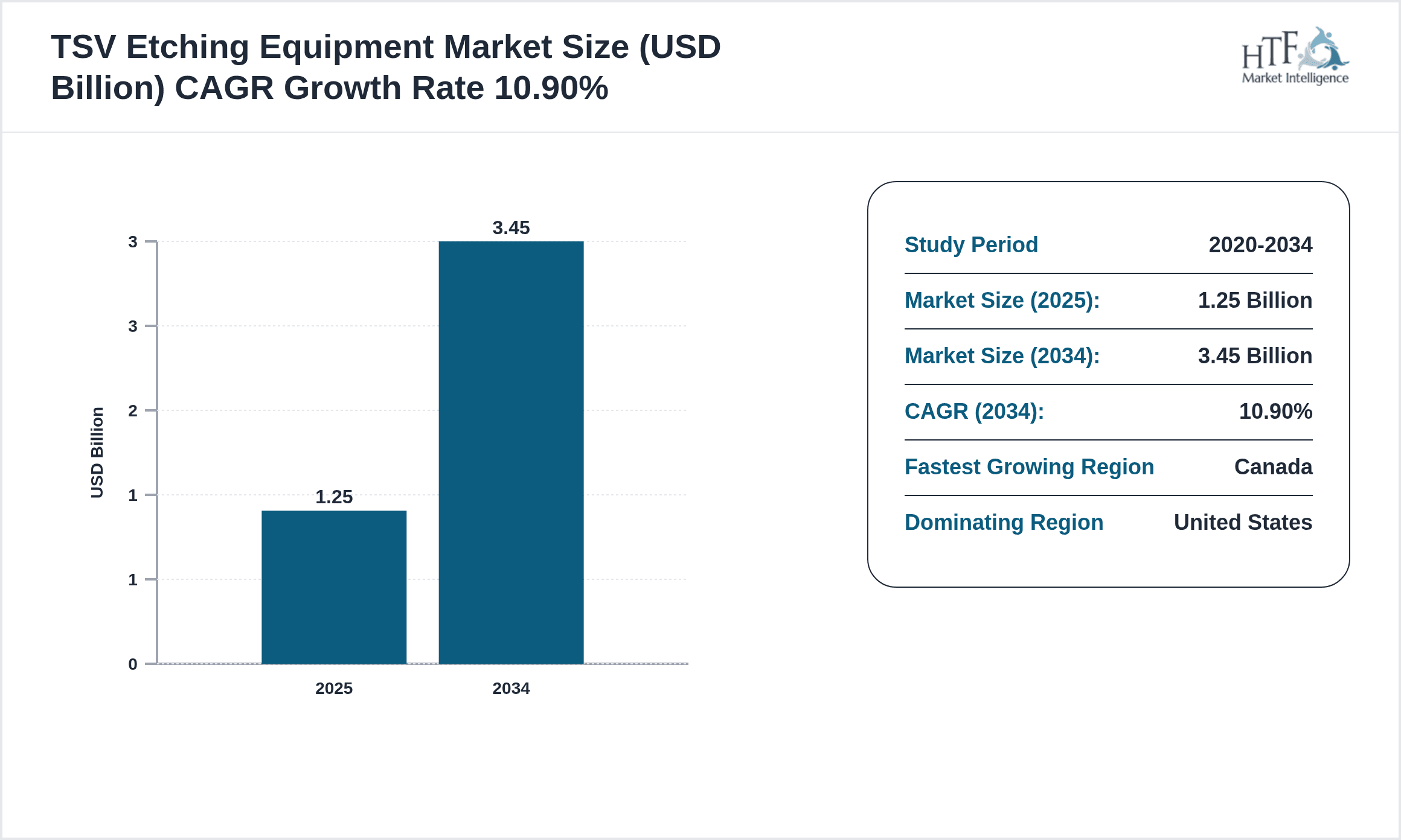
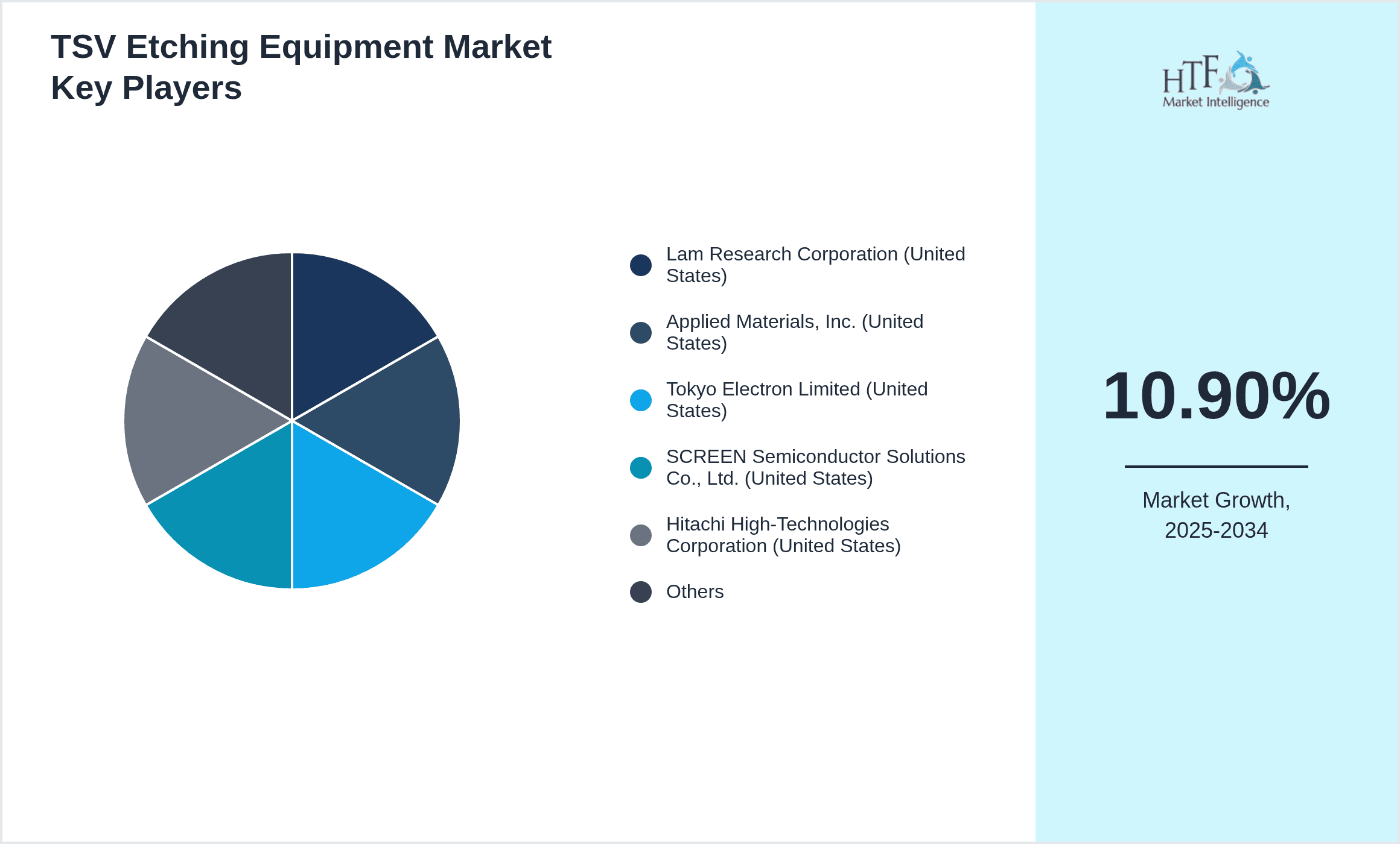
- •Market highlights include a projected CAGR of 10.9% from 2024 to 2034, with the market size expected to reach USD 3.45 Billion by 2034 from USD 1.25 Billion in 2024. Dry etching holds the leading product type position due to its precision and scalability, while plasma etching is the fastest growing type driven by technological innovations. Semiconductor packaging remains the dominant application segment, supported by strong demand in the United States. Canada is identified as the fastest growing regional market within North America, benefiting from increased investment in semiconductor fabrication facilities. The market growth is complemented by rising R&D activities and government initiatives promoting semiconductor manufacturing competitiveness.
- •The value proposition of the North America TSV Etching Equipment Market lies in its critical contribution to the semiconductor fabrication process, enabling manufacturers to achieve miniaturization and enhanced device performance. This market is strategically important for industries reliant on advanced electronics, including automotive, aerospace, and consumer electronics. Stakeholders benefit from high-precision etching technology that supports the development of 3D integrated circuits, facilitating faster, smaller, and more energy-efficient devices. The market's growth potential also attracts investments focusing on innovation, sustainability, and supply chain resilience. Overall, the TSV etching equipment market serves as a foundational technology segment driving the evolution of semiconductor manufacturing in North America.
Competitive Landscape
The North America TSV Etching Equipment Market is characterized by intense competition among established global and regional players focusing on innovation, strategic partnerships, and technological differentiation. Companies invest heavily in R&D to enhance equipment precision, efficiency, and throughput, catering to the evolving demands of semiconductor fabs. Competitive strategies include developing plasma etching and dry etching technologies with better control and lower defect rates. Market positioning hinges on the ability to provide customized solutions aligned with customer requirements, including integration with other wafer fabrication steps. Rivalry is further intensified by the entry of specialized startups and technology providers offering niche solutions. Mergers and acquisitions are common to consolidate technology portfolios and expand market reach. Pricing strategies balance between premium advanced technology offerings and cost-effective solutions for mid-tier customers. Distribution channels and after-sales services also contribute to competitive advantage. Overall, the market exhibits dynamic competitive behavior driven by innovation cycles and the semiconductor industry's growth trajectory.
Leading Companies in North America TSV Etching Equipment Market
- •Lam Research Corporation (United States)
- •Applied Materials, Inc. (United States)
- •Tokyo Electron Limited (United States)
- •SCREEN Semiconductor Solutions Co., Ltd. (United States)
- •Hitachi High-Technologies Corporation (United States)
- •Plasma-Therm LLC (United States)
- •Oxford Instruments plc (United States)
- •Nordson Corporation (United States)
- •Veeco Instruments Inc. (United States)
- •Advanced Micro-Fabrication Equipment Inc. (AMEC) (United States)
- •Semitool, Inc. (United States)
- •SPTS Technologies Ltd. (United States)
- •Cohu, Inc. (United States)
- •MKS Instruments, Inc. (United States)
- •Asahi Glass Co., Ltd. (United States)
- •Entegris, Inc. (United States)
- •Kurt J. Lesker Company (United States)
- •Plasma Etch, Inc. (United States)
- •Veeco Instruments Inc. (United States)
- •Molecular Imprints, Inc. (United States)
- •Technic, Inc. (United States)
- •AMAT (Applied Materials) (United States)
- •Hitachi High-Tech Analytical Science (United States)
- •Canon Anelva Corporation (United States)
- •Veeco Instruments Inc. (United States)

Market Breakdown
- •By Type
- ◦Wet Etching Equipment
- ◦Dry Etching Equipment
- ◦Plasma Etching Equipment
- ◦Chemical Etching Equipment
- ◦Reactive Ion Etching Equipment
- •By Application
- ◦Semiconductor Packaging
- ◦MEMS Devices
- ◦Photonics
- ◦Power Electronics
- ◦Sensors
- •By End-User Industry
- ◦Semiconductor Manufacturers
- ◦Automotive Electronics
- ◦Consumer Electronics
- ◦Aerospace & Defense
- •By Distribution Channel
- ◦Direct Sales
- ◦Third-Party Distributors
- ◦Online Platforms
Growth Dynamics
- •Rising demand for miniaturized and high-performance semiconductor devices in North America is a primary growth driver, pushing the adoption of advanced TSV etching equipment that offers higher precision and throughput for 3D IC fabrication.
- •Technological advancements such as plasma etching and reactive ion etching are enabling more efficient wafer processing, reducing defects, and increasing yield, which stimulates market growth and attracts investments from semiconductor fabs.
- •Government initiatives and incentives to strengthen domestic semiconductor manufacturing capacity in the United States and Canada are accelerating capital expenditures on equipment, thus boosting the TSV etching equipment market.
- •Growing adoption of TSV technology in emerging applications like power electronics and sensors expands the market scope beyond traditional semiconductor packaging, driving new demand segments.
- •Increasing focus on sustainable manufacturing practices encourages equipment providers to develop energy-efficient and environmentally friendly TSV etching systems, aligning with industry regulations and corporate responsibility goals.

Market Trends
- •The integration of AI and machine learning technologies into TSV etching equipment enhances process monitoring and control, improving precision and reducing operational downtime in semiconductor fabs.
- •Shift towards plasma etching methods is gaining momentum due to their superior anisotropic etching capabilities and compatibility with advanced semiconductor materials, leading to increased market share.
- •Collaborative partnerships between equipment manufacturers and semiconductor foundries are becoming common to co-develop customized etching solutions tailored to specific process requirements.
- •Increased emphasis on supply chain resilience post-pandemic is encouraging North American fabs to source TSV etching equipment from regional suppliers, boosting local market growth.
- •Environmental regulations are driving trends towards reducing chemical usage and waste in TSV etching processes, prompting innovation in eco-friendly etching technologies.
Market Opportunities
- •Expansion of semiconductor fabrication facilities in Canada presents a lucrative opportunity for TSV etching equipment suppliers to establish a stronger foothold in this growing market segment.
- •Development of next-generation 3D ICs requiring complex TSV structures creates demand for advanced etching equipment capable of handling diverse material stacks and geometries.
- •Emerging applications in automotive electronics, particularly electric vehicles, offer significant growth potential for TSV etching equipment tailored to power devices and sensors.
- •Adoption of automation and Industry 4.0 practices in semiconductor fabs opens avenues for equipment suppliers to integrate smart features and remote diagnostics in TSV etching systems.
- •Collaborations with research institutions to develop novel etching chemistries and plasma sources can lead to innovative product offerings and market differentiation.
Market Challenges
- •High capital expenditure required for advanced TSV etching equipment limits adoption among small and mid-sized semiconductor manufacturers, restraining market growth.
- •Complexity in process integration and the need for specialized technical expertise to operate and maintain TSV etching systems pose operational challenges for end-users.
- •Stringent environmental and safety regulations around chemical usage and waste disposal increase compliance costs for equipment manufacturers and users.
- •Supply chain disruptions affecting critical components such as plasma sources and control electronics can lead to delayed equipment deliveries and impact market dynamics.
- •Rapid technological obsolescence due to fast-paced semiconductor advancements necessitates continuous innovation, pressuring companies to invest heavily in R&D.
Regulatory Framework
- •From 2019 to 2024, the Environmental Protection Agency (EPA) in the United States has enforced stricter emissions and chemical handling standards for semiconductor manufacturing equipment, compelling TSV etching equipment providers to innovate eco-friendly processes.
- •The Occupational Safety and Health Administration (OSHA) updated workplace safety regulations in 2021, requiring enhanced operator safety protocols and equipment features to minimize exposure to hazardous chemicals during TSV etching.
- •Canada introduced the Canadian Environmental Protection Act amendments in 2023, emphasizing reduction of hazardous waste in manufacturing, impacting TSV etching equipment design and chemical usage.
- •The United States Department of Commerce implemented export control regulations in 2022 affecting semiconductor manufacturing equipment, including TSV etching systems, to protect national security interests.
- •State-level regulations in California and New York have introduced additional compliance requirements for air quality and chemical safety specific to semiconductor fabrication facilities, influencing TSV etching equipment deployment.
Market Intelligence
- •15th January 2025, Lam Research Corporation announced the launch of its new plasma etching system tailored for TSV manufacturing, featuring advanced process control and reduced chemical consumption aimed at improving yield and sustainability in semiconductor fabs across North America. This innovation targets the growing demand for high-density 3D IC structures and positions Lam Research as a technology leader in TSV etching solutions. The product integrates AI-driven diagnostics to optimize etching precision and minimize downtime, aligning with industry trends towards automation and environmental compliance. Source: Official company press release.
- •8th March 2025, Applied Materials, Inc. unveiled a next-generation dry etching platform designed to support advanced semiconductor packaging applications, including MEMS and photonics. The system offers enhanced anisotropic etching capabilities and real-time process monitoring, enabling fabs to reduce defects and improve throughput. This launch reflects Applied Materials' strategic focus on expanding its TSV etching equipment portfolio to capture increased market demand in North America. The platform is expected to accelerate adoption of 3D IC technologies in automotive and consumer electronics sectors. Source: Corporate announcement.
- •22nd May 2024, Plasma-Therm LLC entered a strategic partnership with a leading semiconductor foundry in Canada to co-develop customized plasma etching solutions for power electronics manufacturing. This collaboration aims to optimize TSV etching processes for higher efficiency and lower operational costs, leveraging Plasma-Therm’s expertise in plasma technology and the foundry's production scale. The partnership is anticipated to strengthen Plasma-Therm’s presence in the North American market and cater to emerging EV semiconductor applications. Source: Industry publication.
- •10th October 2024, SCREEN Semiconductor Solutions Co., Ltd. expanded its North American operations by opening a new R&D center focused on TSV etching equipment innovation. This facility is dedicated to developing next-generation etching technologies that address challenges in material compatibility and process integration, supporting semiconductor manufacturers’ transition to advanced packaging. The expansion underscores SCREEN’s commitment to local market growth and collaborative development with regional semiconductor ecosystems. Source: Company website.
Regional Outlook
The United States currently holds a significant share of the market, primarily due to several key factors: increasing consumption rates, a burgeoning population, and robust economic momentum. These elements collectively drive demand, positioning this region as a leader in the market. On the other hand, Canada is rapidly emerging as the fastest-growing area within the industry. This remarkable growth can be attributed to swift infrastructure development, the expansion of various industrial sectors, and a marked increase in consumer demand. These dynamics make this region a crucial player in shaping future market growth.
In our report, we cover a comprehensive analysis of the following regions and countries:
- United States
- Canada
- Mexico
| Feature | Details |
|---|---|
| Base Year Market Size | USD 1.25 Billion |
| Forecast Year Market Size | USD 3.45 Billion |
| CAGR | 10.9% |
| Forecast Period | 2026 to 2033 |
| YoY Growth | 10.4% |
| Scope of Report | Market is segmented by Type (Wet Etching Equipment, Dry Etching Equipment, Plasma Etching Equipment, Chemical Etching Equipment, Reactive Ion Etching Equipment), Application (Semiconductor Packaging, MEMS Devices, Photonics, Power Electronics, Sensors), End-User Industry (Semiconductor Manufacturers, Automotive Electronics, Consumer Electronics, Aerospace & Defense), Distribution Channel (Direct Sales, Third-Party Distributors, Online Platforms) |
| Regions Covered | United States, Canada, Mexico |
| Key Companies | Lam Research Corporation (United States), Applied Materials, Inc. (United States), Tokyo Electron Limited (United States), SCREEN Semiconductor Solutions Co., Ltd. (United States), Hitachi High-Technologies Corporation (United States), Plasma-Therm LLC (United States), Oxford Instruments plc (United States), Nordson Corporation (United States), Veeco Instruments Inc. (United States), Advanced Micro-Fabrication Equipment Inc. (AMEC) (United States), Semitool, Inc. (United States), SPTS Technologies Ltd. (United States), Cohu, Inc. (United States), MKS Instruments, Inc. (United States), Asahi Glass Co., Ltd. (United States), Entegris, Inc. (United States), Kurt J. Lesker Company (United States), Plasma Etch, Inc. (United States), Veeco Instruments Inc. (United States), Molecular Imprints, Inc. (United States), Technic, Inc. (United States), AMAT (Applied Materials) (United States), Hitachi High-Tech Analytical Science (United States), Canon Anelva Corporation (United States), Veeco Instruments Inc. (United States) |
North America TSV Etching Equipment Market Size, Growth & Revenue 2024-2034 - Table of Contents
Frequently Asked Questions (FAQ):
The Compact Track Loaders market is projected to grow at a CAGR of 6.8% from 2025 to 2030, driven by increasing demand in construction and agricultural sectors.
North America currently leads the market with approximately 45% market share, followed by Europe at 28% and Asia-Pacific at 22%. The remaining regions account for 5% of the global market.
Key growth drivers include increasing construction activities, rising demand for versatile equipment in agriculture, technological advancements in track loader design, and growing preference for compact equipment in urban construction projects.