
Asia-Pacific Atomic Layer Deposition Equipment Market Size, Growth & Revenue 2025-2034
Asia-Pacific Atomic Layer Deposition Equipment for Advanced Packaging Market is segmented by ALD Equipment Type (Thermal Atomic Layer Deposition Equipment, Plasma-Enhanced Atomic Layer Deposition Equipment, Spatial Atomic Layer Deposition Equipment, Atomic Layer Deposition Precursors, Atomic Layer Deposition Reactors), Advanced Packaging Application (Logic Devices, Memory Devices, RF Devices, Power Devices, Sensors), Process Integration Stage (Wafer-Level Packaging, Fan-Out Packaging, Chip-Scale Packaging, System-in-Package (SiP)), Deployment Model (On-Premise Installation, Turnkey Equipment Solutions, Custom ALD Tool Integration), and Geography (Asai-Pacific)
Pricing
Report Overview
Executive Summary
- •The Asia-Pacific Atomic Layer Deposition (ALD) Equipment market for Advanced Packaging is an essential segment of the semiconductor manufacturing ecosystem, focusing on equipment that enables highly conformal and precise thin film deposition critical for advanced semiconductor packaging technologies. This market covers a range of ALD technologies such as thermal ALD, plasma-enhanced ALD, and spatial ALD, each providing unique advantages in deposition uniformity, throughput, and material compatibility. The equipment is predominantly utilized in advanced packaging applications including logic devices, memory devices, RF devices, power devices, and sensors, supporting the expanding semiconductor content in consumer electronics, automotive, telecommunications, and industrial sectors. Asia-Pacific leads this market due to its extensive semiconductor manufacturing infrastructure, with China, Japan, South Korea, India, and Southeast Asia as key contributors. Market growth is driven by the increasing complexity of semiconductor devices, the shift towards miniaturization, and the demand for higher performance and energy efficiency in electronic components. Despite challenges such as high equipment costs and technological complexities, ongoing R&D and investments in spatial ALD and plasma-enhanced ALD are unlocking new growth avenues. This market report provides a detailed analysis of market size, growth drivers, opportunities, challenges, regional dynamics, regulatory environment, and competitive landscape specific to Asia-Pacific, offering valuable insights for stakeholders involved in the semiconductor equipment industry.
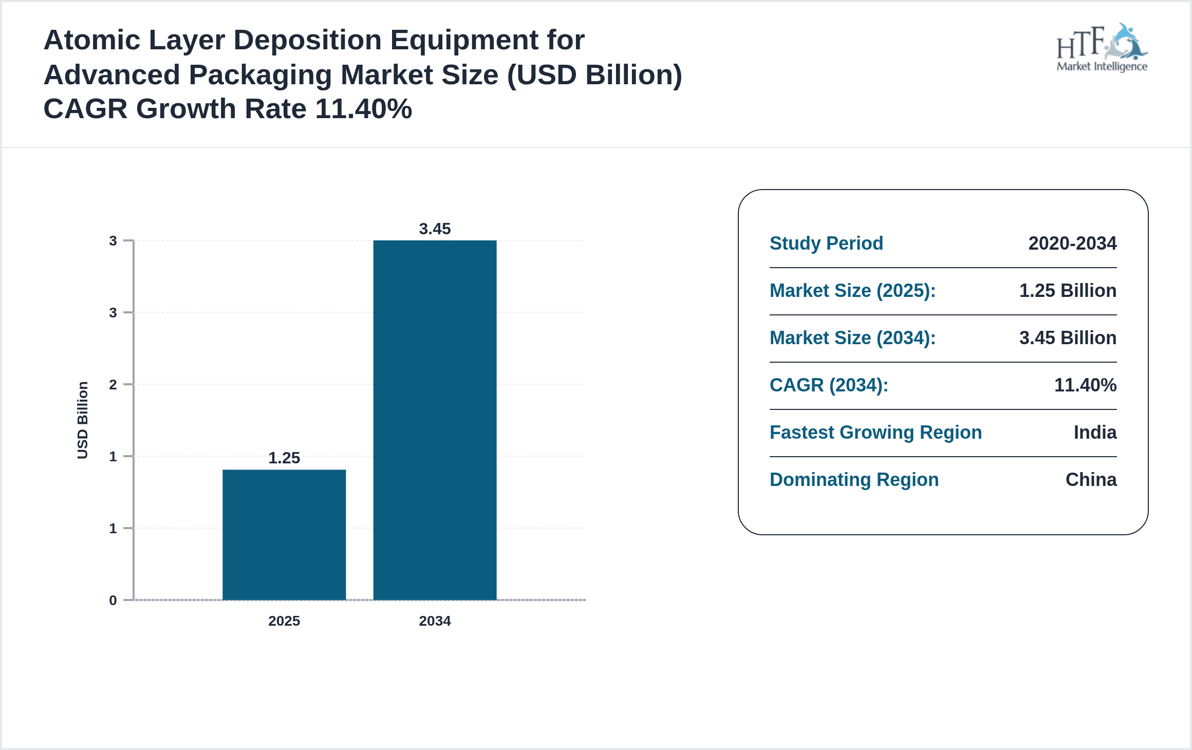
- •Key market highlights include a base market size of USD 1.25 Billion in 2025, projected to grow to USD 3.45 Billion by 2034, reflecting a robust CAGR of 11.4%. China remains the dominating country with a 45% market share, driven by its extensive semiconductor fabrication capacity and government support. India emerges as the fastest-growing country with a CAGR of 15.2%, fueled by increasing investments in semiconductor manufacturing and advanced packaging capabilities. The leading product type is Thermal ALD Equipment, favored for its maturity and reliability, while Spatial ALD Equipment is the fastest growing, offering enhanced throughput for high-volume production. The market experiences consistent year-on-year growth averaging 11.0%, supported by rising demand for consumer electronics, 5G infrastructure, and automotive semiconductors. Industry players focus on technological innovations, strategic partnerships, and capacity expansions to capitalize on the growth opportunities in the Asia-Pacific region.
- •The value proposition of the Asia-Pacific Atomic Layer Deposition Equipment market lies in its critical role in enabling the next generation of semiconductor devices with improved performance, energy efficiency, and form factor. Advanced packaging techniques require precise and reliable ALD processes to deposit ultra-thin films such as dielectrics and metal oxides that enhance device functionality and longevity. This market's strategic importance is underscored by the semiconductor industry's shift towards heterogeneous integration and system-in-package solutions, where ALD equipment provides the necessary process control and material versatility. Stakeholders including equipment manufacturers, semiconductor foundries, and materials suppliers benefit from the growing demand for ALD tools tailored to advanced packaging needs. Furthermore, government initiatives in Asia-Pacific aimed at bolstering semiconductor self-reliance and innovation fuel investments and collaborations within this market, making it a pivotal segment for regional technology leadership and economic growth.
Competitive Landscape
The Asia-Pacific Atomic Layer Deposition Equipment market for Advanced Packaging exhibits a competitive environment characterized by a mix of global technology leaders and regional specialists focusing on innovation, strategic partnerships, and capacity expansion. Market players employ diverse strategies including continuous R&D to enhance equipment throughput, precision, and compatibility with emerging semiconductor materials. Competitive positioning is influenced by the ability to provide turnkey solutions integrating ALD equipment with advanced process control systems. Companies differentiate through product customization for specific advanced packaging applications such as logic and memory devices, and by offering comprehensive after-sales services to semiconductor manufacturers. Mergers and acquisitions have been modest but strategically targeted to acquire complementary technologies and expand geographic reach in Asia-Pacific. Pricing strategies balance between premium high-performance tools and cost-effective solutions for mature segments, while distribution channels leverage direct customer engagement and collaborations with semiconductor fabs. Technology adoption trends highlight a shift towards spatial ALD for increased production efficiency and plasma-enhanced ALD for material innovation. Market entry barriers include high capital requirements, technical expertise, and intellectual property considerations, which sustain the competitive advantage of established players. Overall, the competitive landscape is dynamic, with future trends expected to focus on integration of AI-driven process optimization and expansion into emerging markets within Asia-Pacific.
Leading Companies in Atomic Layer Deposition Equipment for Advanced Packaging Market
- •ASM International NV (Netherlands)
- •Lam Research Corporation (United States)
- •Tokyo Electron Limited (Japan)
- •Applied Materials, Inc. (United States)
- •Kokusai Electric Corporation (Japan)
- •Veeco Instruments Inc. (United States)
- •Beneq Oy (Finland)
- •Hitachi High-Tech Corporation (Japan)
- •Picosun Oy (Finland)
- •SENTECH Instruments GmbH (Germany)
- •Oxford Instruments plc (United Kingdom)
- •Ultratech, Inc. (United States)
- •Mechatro, Inc. (South Korea)
- •Semes Co., Ltd. (South Korea)
- •Wonik IPS Co., Ltd. (South Korea)
- •Plasma-Therm LLC (United States)
- •CVD Equipment Corporation (United States)
- •Kurt J. Lesker Company (United States)
- •Nuflare Technology, Inc. (Japan)
- •Jusung Engineering Co., Ltd. (South Korea)
- •Suzhou Huanan Microelectronics Co., Ltd. (China)
- •Mantis Deposition Ltd. (United Kingdom)
- •Advanced Micro-Fabrication Equipment Inc. China (AMEC) (China)
- •Ebara Corporation (Japan)
- •Shin-Etsu Chemical Co., Ltd. (Japan)
Market Breakdown
- •By ALD Equipment Type
- ◦Thermal Atomic Layer Deposition Equipment
- ◦Plasma-Enhanced Atomic Layer Deposition Equipment
- ◦Spatial Atomic Layer Deposition Equipment
- ◦Atomic Layer Deposition Precursors
- ◦Atomic Layer Deposition Reactors
- •By Advanced Packaging Application
- ◦Logic Devices
- ◦Memory Devices
- ◦RF Devices
- ◦Power Devices
- ◦Sensors
- •By Process Integration Stage
- ◦Wafer-Level Packaging
- ◦Fan-Out Packaging
- ◦Chip-Scale Packaging
- ◦System-in-Package (SiP)
- •By Deployment Model
- ◦On-Premise Installation
- ◦Turnkey Equipment Solutions
- ◦Custom ALD Tool Integration
Growth Dynamics
The Asia-Pacific Atomic Layer Deposition Equipment market for Advanced Packaging is propelled by the rapid expansion of semiconductor manufacturing infrastructure across the region, particularly in China and India. Growing demand for miniaturized, high-performance semiconductor devices in consumer electronics, automotive, and telecommunications sectors is driving adoption of advanced packaging technologies that require precise ALD processes. Innovations in spatial ALD equipment are addressing throughput challenges, enabling mass production scalability. Government initiatives promoting semiconductor self-reliance and investment incentives in countries like China, South Korea, and India further accelerate market growth. Moreover, the increasing complexity of 5G, IoT, and AI applications necessitates ultra-thin film depositions with atomic-level control, amplifying the need for cutting-edge ALD equipment. Industry collaboration among equipment manufacturers and foundries fosters technology advancements and process optimizations, enhancing overall market momentum and creating a robust foundation for sustained growth through the forecast period.

Market Trends
The Asia-Pacific market is witnessing a significant shift towards spatial ALD technology due to its superior throughput capabilities essential for high-volume manufacturing in advanced packaging. Additionally, integration of AI and machine learning algorithms for real-time process monitoring and defect reduction is gaining traction among equipment manufacturers and semiconductor fabs. There is a growing trend of localization with increased domestic production of ALD equipment components to reduce supply chain dependencies. Sustainability considerations are influencing equipment design, focusing on energy efficiency and reduced precursor wastage. Collaborative R&D efforts between semiconductor foundries and ALD tool providers are fostering rapid innovation cycles, enabling faster adoption of emerging materials such as high-k dielectrics and metal oxides in packaging applications.

Market Opportunities
Asia-Pacific offers substantial opportunities driven by the burgeoning semiconductor ecosystems in India and Southeast Asia, which are rapidly developing advanced packaging capabilities. The rising adoption of electric vehicles and 5G infrastructure also opens new application areas for ALD equipment in power devices and RF components. Investments in spatial ALD and plasma-enhanced ALD technologies enable equipment providers to tap into markets demanding higher throughput and novel material depositions. Expanding collaborations with local semiconductor manufacturers and government-supported initiatives to build semiconductor fabs create conducive environments for market penetration. Furthermore, increasing demand for heterogeneous integration and system-in-package solutions presents opportunities for customized ALD tooling and process innovations tailored to advanced packaging requirements.
Market Challenges
High capital expenditure and operational complexity associated with ALD equipment pose significant barriers to entry and adoption, particularly for emerging semiconductor producers in Asia-Pacific. The technological sophistication required for process optimization and material compatibility demands specialized expertise, limiting widespread deployment. Supply chain disruptions and precursor material availability can impact production schedules and equipment utilization. Moreover, the rapid pace of semiconductor technology evolution requires continuous equipment upgrades, which can be cost-prohibitive for some manufacturers. Regulatory compliance related to chemical handling and environmental standards also adds to operational challenges, necessitating rigorous safety and sustainability measures. These factors combined create a challenging environment that requires strategic planning and investment to navigate effectively.
Regulatory Framework
Between 2020 and 2025, Asia-Pacific jurisdictions implemented stringent regulations governing chemical usage, emissions, and safety standards in semiconductor manufacturing to minimize environmental impact and ensure worker safety. Japan and South Korea introduced enhanced chemical handling protocols mandating certification and training for personnel operating ALD equipment. China enacted policies focusing on reducing volatile organic compound (VOC) emissions in semiconductor fabs, requiring equipment upgrades to meet compliance. India established regulatory frameworks promoting green manufacturing practices, incentivizing adoption of energy-efficient ALD tools. Additionally, cross-border trade regulations influenced import-export dynamics of ALD equipment and precursor chemicals, affecting supply chain strategies. These regulatory developments compel manufacturers to prioritize environmental sustainability and safety in equipment design and operation, fostering innovation in low-waste and energy-efficient ALD solutions while ensuring compliance with evolving standards.
Market Intelligence
- •15th February 2025, ASM International NV announced the launch of its latest thermal ALD equipment designed specifically for advanced packaging applications, featuring enhanced throughput and improved film uniformity across large substrates. The new tool integrates AI-driven process control to minimize defects and optimize precursor usage, targeting major semiconductor fabs in China and South Korea. This launch aims to address the increasing demand for higher performance and miniaturized devices in the Asia-Pacific region, strengthening ASM's market position. Source: ASM International official press release.
- •10th May 2025, Tokyo Electron Limited unveiled a plasma-enhanced ALD system that supports novel materials for next-generation power devices and RF applications. The system provides superior control over film properties, enabling semiconductor manufacturers to meet strict performance and reliability standards. This innovation responds to growing requirements in 5G infrastructure and electric vehicle semiconductors across Asia-Pacific markets, including India and Southeast Asia. Tokyo Electron's strategic focus on regional collaboration with local foundries aims to accelerate adoption and customization. Source: Tokyo Electron corporate announcement.
- •22nd August 2024, Semes Co., Ltd., a South Korean equipment manufacturer, announced a $150 million investment to expand its ALD equipment production capacity targeting advanced packaging markets. The expansion includes R&D centers focused on spatial ALD technology to deliver higher throughput tools suitable for volume manufacturing in Asia-Pacific. This investment aligns with increasing semiconductor fabrication investments in China and India and aims to capture emerging growth opportunities. The company also plans to enhance after-sales services and technical support to strengthen customer relationships. Source: Semes official news release.
- •Market Intelligence: Recent developments and industry insights are being monitored. For the latest updates, consult official company announcements and industry publications.
Regional Outlook
The China currently holds a significant share of the market, primarily due to several key factors: increasing consumption rates, a burgeoning population, and robust economic momentum. These elements collectively drive demand, positioning this region as a leader in the market. On the other hand, India is rapidly emerging as the fastest-growing area within the industry. This remarkable growth can be attributed to swift infrastructure development, the expansion of various industrial sectors, and a marked increase in consumer demand. These dynamics make this region a crucial player in shaping future market growth.
In our report, we cover a comprehensive analysis of the following regions and countries:
| Feature | Details |
|---|---|
| Base Year Market Size | USD 1.25 Billion |
| Forecast Year Market Size | USD 3.45 Billion |
| CAGR | 11.4% |
| Forecast Period | 2026 to 2033 |
| YoY Growth | 11% |
| Scope of Report | Market is segmented by ALD Equipment Type (Thermal Atomic Layer Deposition Equipment, Plasma-Enhanced Atomic Layer Deposition Equipment, Spatial Atomic Layer Deposition Equipment, Atomic Layer Deposition Precursors, Atomic Layer Deposition Reactors), Advanced Packaging Application (Logic Devices, Memory Devices, RF Devices, Power Devices, Sensors), Process Integration Stage (Wafer-Level Packaging, Fan-Out Packaging, Chip-Scale Packaging, System-in-Package (SiP)), Deployment Model (On-Premise Installation, Turnkey Equipment Solutions, Custom ALD Tool Integration) |
| Key Companies | ASM International NV (Netherlands), Lam Research Corporation (United States), Tokyo Electron Limited (Japan), Applied Materials, Inc. (United States), Kokusai Electric Corporation (Japan), Veeco Instruments Inc. (United States), Beneq Oy (Finland), Hitachi High-Tech Corporation (Japan), Picosun Oy (Finland), SENTECH Instruments GmbH (Germany), Oxford Instruments plc (United Kingdom), Ultratech, Inc. (United States), Mechatro, Inc. (South Korea), Semes Co., Ltd. (South Korea), Wonik IPS Co., Ltd. (South Korea), Plasma-Therm LLC (United States), CVD Equipment Corporation (United States), Kurt J. Lesker Company (United States), Nuflare Technology, Inc. (Japan), Jusung Engineering Co., Ltd. (South Korea), Suzhou Huanan Microelectronics Co., Ltd. (China), Mantis Deposition Ltd. (United Kingdom), Advanced Micro-Fabrication Equipment Inc. China (AMEC) (China), Ebara Corporation (Japan), Shin-Etsu Chemical Co., Ltd. (Japan) |
Asia-Pacific Atomic Layer Deposition Equipment Market Size, Growth & Revenue 2025-2034 - Table of Contents
Multidisciplinary researcher with 10+ years of experience uncovering insights across diverse domains focused on uncovering insights that drive informed decisions.
Frequently Asked Questions (FAQ):
The Compact Track Loaders market is expected to see value worth 5.3 Billion in 2025.
North America currently leads the market with approximately 45% market share, followed by Europe at 28% and Asia-Pacific at 22%. The remaining regions account for 5% of the global market.
Key growth drivers include increasing construction activities, rising demand for versatile equipment in agriculture, technological advancements in track loader design, and growing preference for compact equipment in urban construction projects.