
Asia-Pacific BCD Process Wafer Foundry Market Size, Growth & Revenue 2025-2034
Asia-Pacific BCD Process Wafer Foundry Market is segmented by BCD Technology Node (BCD 0.13 Micron Process, BCD 0.18 Micron Process, BCD 0.35 Micron Process, BCD 0.5 Micron Process, BCD 0.8 Micron Process), Semiconductor Application (Power Management ICs, RF Devices, Analog Circuits, Mixed-Signal ICs, Micro-Electromechanical Systems (MEMS)), Service Type (Turnkey Foundry Services, Pure-Play Foundry Services, Custom Foundry Services, Volume Production Services), Manufacturing Location (In-House Fabrication, Outsourced Fabrication, Joint Venture Facilities), and Geography (Japan, China, Southeast Asia, India, Australia, South Korea, Others)
Pricing
Report Overview
Executive Summary
The Asia-Pacific BCD Process Wafer Foundry market is a critical segment within the semiconductor manufacturing industry, focusing on the production of Bipolar-CMOS-DMOS wafers that integrate multiple transistor types on a single substrate. This market serves diverse applications including power management integrated circuits, radio frequency devices, analog and mixed-signal circuits, and micro-electromechanical systems, which are pivotal in automotive electronics, telecommunications, consumer electronics, and industrial automation. The value chain comprises raw material providers, wafer foundries specializing in BCD technology, design firms, and end users who demand high-performance and energy-efficient solutions. Technological advancements and increasing demand for compact, high-voltage, and high-current semiconductor devices are driving the growth of this market. Moreover, the Asia-Pacific region, led by countries such as China, India, Japan, and South Korea, has emerged as a dominant manufacturing hub due to its advanced fabrication capabilities and robust supply chain ecosystems. This market is characterized by rapid innovation, stringent quality standards, and strategic collaborations between foundries and semiconductor design houses. The expanding automotive electronics sector and the proliferation of IoT devices further contribute to the rising adoption of BCD process wafers, underscoring the market's strategic importance across multiple industries. Over the forecast period, continuous investments in research and development, alongside government incentives, are expected to sustain the market's growth trajectory, enhancing the region's global semiconductor competitiveness.

Competitive Landscape
The competitive environment within the Asia-Pacific BCD Process Wafer Foundry market is shaped by a combination of established multinational semiconductor foundries and emerging regional players. Market dynamics are influenced by rapid technological advancements, with companies investing heavily in next-generation BCD process nodes to achieve superior device performance and energy efficiency. Competitive strategies include strategic partnerships with semiconductor design firms, alliances for technology sharing, and expansion of fabrication capacities to meet growing demand. Market positioning is often determined by a company's ability to provide customized solutions tailored to specific industry applications such as automotive and industrial electronics. Innovation is a key differentiator, with leading foundries focusing on integrating advanced process technologies, enhancing wafer yields, and reducing production costs. Mergers and acquisitions have been instrumental in consolidating market presence and expanding technological capabilities, enabling companies to broaden their product portfolios and geographical reach. Pricing strategies are competitive but reflect the high value added by advanced BCD wafers. Distribution channels are increasingly optimized through regional hubs to ensure timely delivery and customer support. Adoption of automation and digital manufacturing techniques is enhancing operational efficiencies. Barriers to entry remain high due to significant capital expenditure requirements and the need for advanced technological expertise. Regional competition is robust, with China and South Korea leading in capacity, while Japan and India are emerging as innovation centers. Future trends suggest intensified focus on sustainable manufacturing practices and integration of AI-driven process controls to maintain competitive advantages.
Leading Companies in BCD Process Wafer Foundry Market
- •TSMC (Taiwan)
- •Samsung Electronics (South Korea)
- •GlobalFoundries (Singapore)
- •SMIC (China)
- •Tower Semiconductor (Israel, with Asia-Pacific operations)
- •United Microelectronics Corporation (UMC) (Taiwan)
- •Vanguard International Semiconductor Corporation (Taiwan)
- •Dongbu HiTek (South Korea)
- •VIS (Vanguard International Semiconductor) (Taiwan)
- •Powerchip Technology Corporation (Taiwan)
- •X-FAB Silicon Foundries (Malaysia, Singapore)
- •Hua Hong Semiconductor (China)
- •Advanced Semiconductor Manufacturing Corporation (China)
- •GlobalWafers (Taiwan)
- •Silterra Malaysia Sdn Bhd (Malaysia)
- •DB HiTek Co., Ltd. (South Korea)
- •SMEE (Shanghai Micro Electronics Equipment Co.) (China)
- •NANIUM S.A. (South Korea/Asia-Pacific presence)
- •JHICC (Japan)
- •Renesas Electronics Corporation (Japan)
- •Tachyum (India, Asia-Pacific operations)
- •SITRI (Semiconductor Manufacturing International Corporation) (China)
- •HCL Technologies (India)
- •SMIC Wuhan (China)
- •SilTerra Malaysia (Malaysia)
Market Breakdown
- •By BCD Technology Node
- ◦BCD 0.13 Micron Process
- ◦BCD 0.18 Micron Process
- ◦BCD 0.35 Micron Process
- ◦BCD 0.5 Micron Process
- ◦BCD 0.8 Micron Process
- •By Semiconductor Application
- ◦Power Management ICs
- ◦RF Devices
- ◦Analog Circuits
- ◦Mixed-Signal ICs
- ◦Micro-Electromechanical Systems (MEMS)
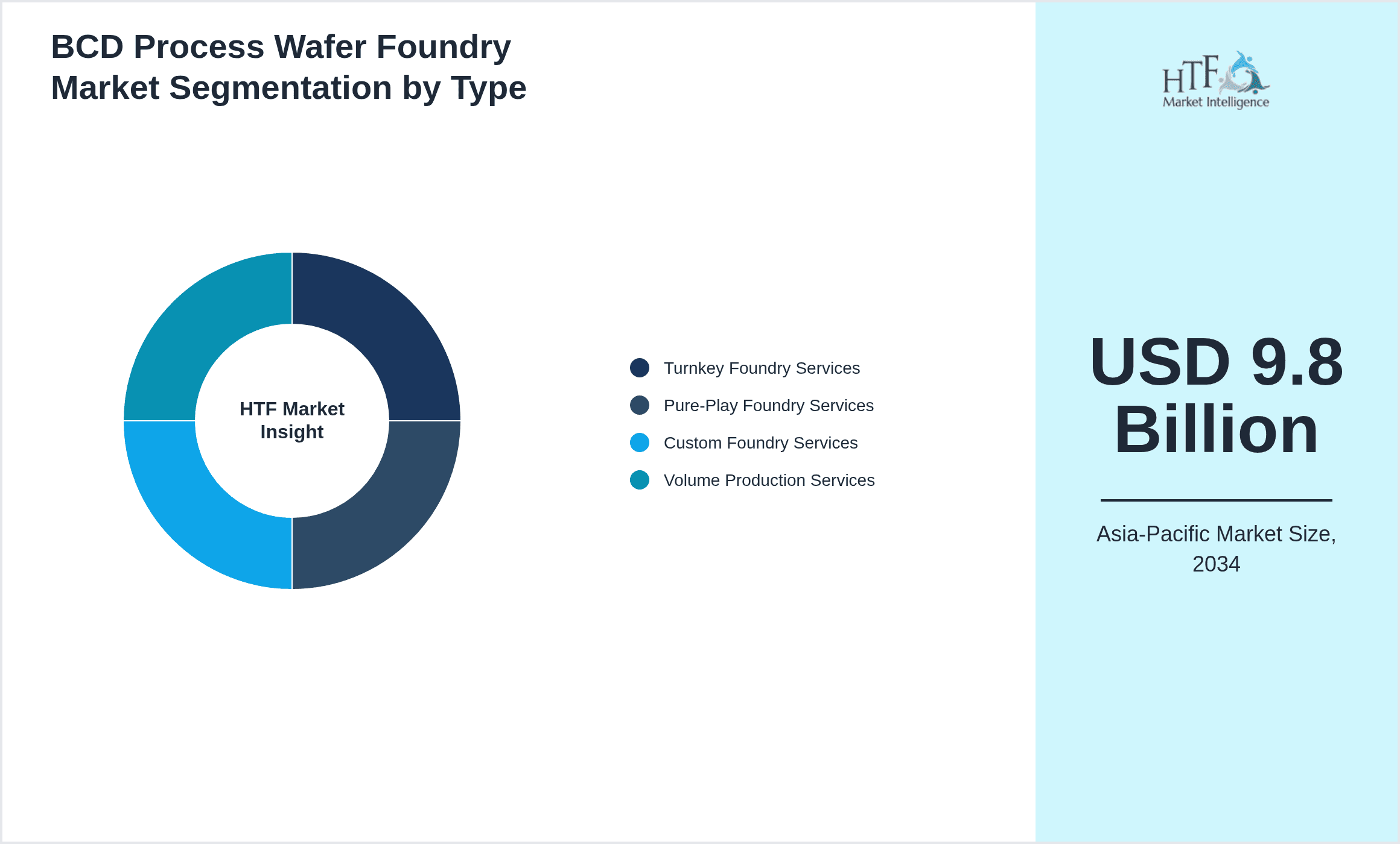
- •By Service Type
- ◦Turnkey Foundry Services
- ◦Pure-Play Foundry Services
- ◦Custom Foundry Services
- ◦Volume Production Services
- •By Manufacturing Location
- ◦In-House Fabrication
- ◦Outsourced Fabrication
- ◦Joint Venture Facilities
Growth Dynamics
- •The Asia-Pacific BCD Process Wafer Foundry market growth is fueled by the rapid expansion of automotive electronics, particularly electric vehicle powertrain components requiring high-voltage and high-current semiconductor devices. Increasing adoption of advanced driver-assistance systems (ADAS) drives demand for reliable BCD wafers with enhanced performance.
- •The proliferation of 5G infrastructure and IoT devices in Asia-Pacific has escalated demand for RF and mixed-signal ICs fabricated using BCD processes, enabling efficient signal processing and power management in compact designs.
- •Government initiatives and subsidies in countries like China, South Korea, and India to boost semiconductor manufacturing capabilities have incentivized expansion of foundry capacities specializing in BCD technology nodes, stimulating market growth.
- •Rising consumer electronics demand, including smartphones and wearable devices, that integrate analog and power management ICs based on BCD technology contributes significantly to the market’s robust growth trajectory.
- •Technological advancements in BCD process integration, such as enhanced transistor structures and miniaturization, improve device efficiency and reliability, attracting increased adoption across industrial automation sectors.
- •The growing trend towards energy-efficient electronics and green technologies encourages manufacturers to utilize BCD wafers optimized for lower power consumption and higher thermal stability, further propelling market expansion.
- •Investment in R&D by key foundries to develop advanced BCD process nodes ensures sustained innovation and competitive positioning, fostering steady market growth throughout the forecast period.
Market Trends
- •Integration of BCD technology with advanced CMOS process nodes is trending, enabling highly integrated, multifunctional chips that reduce size and improve power efficiency for mobile and automotive applications.
- •Foundries are increasingly adopting Industry 4.0 practices, including AI-driven process optimization and automation, to enhance wafer yield and reduce production costs in BCD manufacturing.
- •Sustainability trends are influencing foundry operations, with companies investing in eco-friendly manufacturing processes and waste reduction techniques to meet regulatory and consumer expectations.
- •Collaborations between foundries and semiconductor design companies are growing, focusing on co-developing customized BCD solutions tailored to specific end-use applications.
- •Emergence of new applications such as power electronics for renewable energy systems and wearable medical devices is expanding the scope of BCD wafer utilization.
- •Market segmentation is becoming more granular, with foundries offering differentiated BCD process variants to address niche requirements in terms of voltage, current capacity, and integration level.
- •Increasing geopolitical emphasis on semiconductor self-reliance in Asia-Pacific is driving regional capacity expansions and technology upgrades in BCD wafer production.

Market Opportunities
- •Expanding automotive electronics in emerging Asia-Pacific economies presents significant growth opportunities for BCD wafer foundries, particularly with the rise of electric vehicles and ADAS systems requiring specialized semiconductor processes.
- •Increased demand for energy-efficient and high-performance power management ICs across consumer electronics segments opens avenues for foundries to innovate and capture new market share.
- •Strategic partnerships between foundries and fabless semiconductor companies focused on IoT and 5G applications can accelerate market penetration of advanced BCD process technologies.
- •Government support and subsidies in countries like India and China for domestic semiconductor manufacturing offer lucrative opportunities for capacity expansions and technology upgrades within the BCD foundry segment.
- •Emerging markets in Southeast Asia represent untapped potential for BCD wafer adoption in industrial automation and medical devices, encouraging foundries to expand service offerings and regional presence.
- •Advancements in miniaturization and heterogeneous integration provide opportunities for BCD foundries to develop next-generation wafers meeting evolving industry standards and customer demands.
- •Investment in sustainable manufacturing technologies can differentiate foundries and align with increasing regulatory requirements, enhancing competitive advantage and customer appeal.
Market Challenges
- •High capital expenditure requirements for upgrading fabrication facilities to advanced BCD process nodes pose significant barriers to entry and expansion, particularly for smaller foundries.
- •Complexity in integrating bipolar, CMOS, and DMOS transistors on a single wafer demands advanced technical expertise and stringent quality control, limiting the number of capable manufacturers.
- •Supply chain disruptions, including shortages of raw materials and equipment, have impacted production timelines and costs, posing challenges to consistent market supply.
- •Intense competition from global foundries and regional players results in pricing pressures and necessitates continuous innovation to maintain market share.
- •Regulatory compliance with diverse environmental and safety standards across Asia-Pacific countries increases operational complexity and cost for wafer foundries.
- •Talent shortages in semiconductor manufacturing and process engineering fields constrain capacity expansions and technology development initiatives.
- •Intellectual property protection concerns and geopolitical tensions may hinder cross-border collaborations and technology transfer within the Asia-Pacific region.
Regulatory Framework
- •Between 2020 and 2025, several Asia-Pacific countries implemented semiconductor manufacturing policies aimed at strengthening domestic capabilities. China’s 'Made in China 2025' policy, enacted in 2015 and progressively enforced through 2025, mandates local content requirements and incentivizes investments in advanced foundry technologies including BCD processes.
- •South Korea’s Semiconductor Industry Promotion Act (2021) introduced tax incentives and R&D grants targeting fabrication upgrades and green manufacturing practices, supporting compliance with environmental regulations and fostering sustainable growth.
- •India’s National Policy on Electronics (2019) and subsequent amendments up to 2025 provide subsidies and infrastructure support for semiconductor foundries, emphasizing technology transfer and skill development in BCD wafer fabrication.
- •Environmental regulations across Asia-Pacific, including waste management, chemical handling, and emissions standards, have become more stringent, requiring foundries to adopt cleaner manufacturing processes and advanced waste treatment technologies by 2025.
- •Government initiatives such as Japan’s Semiconductor Strategy (2020) promote innovation clusters and international collaboration while enforcing compliance with export control and intellectual property protection frameworks, shaping the regulatory landscape significantly.
Market Intelligence
- •15th January 2025, TSMC announced the commissioning of its advanced BCD process fabrication line in Taiwan, featuring 0.13 micron technology optimized for power management ICs and automotive applications. This new facility aims to increase capacity by 30% and reduce production costs by 15%, positioning TSMC as a leader in Asia-Pacific BCD wafer foundry services. The investment aligns with growing regional demand for high-efficiency semiconductor devices and supports TSMC's strategic goal of expanding its automotive semiconductor portfolio. Source: TSMC Official Press Release
- •8th March 2025, Samsung Electronics unveiled a collaboration with major automotive OEMs in South Korea to develop customized BCD wafers tailored for electric vehicle power modules. The partnership focuses on integrating advanced BCD 0.13 and 0.18 micron nodes to enhance energy efficiency and thermal performance. Samsung plans to leverage its foundry capabilities to support increased demand in the EV sector, reinforcing its position in the Asia-Pacific market. Source: Samsung Newsroom
- •22nd June 2024, SMIC expanded its BCD wafer foundry capacity in Shanghai with the launch of a new 0.18 micron fabrication line aimed at RF and mixed-signal IC production. This expansion responds to rising demand from 5G infrastructure developers in China and Southeast Asia. SMIC’s capacity boost is expected to improve supply chain resilience and market share in the Asia-Pacific region. Source: SMIC Corporate Announcement
- •10th October 2024, GlobalFoundries announced a strategic partnership with an Indian semiconductor design firm to co-develop BCD process wafers optimized for industrial automation and IoT applications. The collaboration focuses on accelerating product development cycles and expanding market reach in India and Southeast Asia. This initiative supports GlobalFoundries’ growth strategy in the Asia-Pacific foundry market segment. Source: GlobalFoundries Press Release
Regional Outlook
The China currently holds a significant share of the market, primarily due to several key factors: increasing consumption rates, a burgeoning population, and robust economic momentum. These elements collectively drive demand, positioning this region as a leader in the market. On the other hand, India is rapidly emerging as the fastest-growing area within the industry. This remarkable growth can be attributed to swift infrastructure development, the expansion of various industrial sectors, and a marked increase in consumer demand. These dynamics make this region a crucial player in shaping future market growth.
In our report, we cover a comprehensive analysis of the following regions and countries:
- Japan
- China
- Southeast Asia
- India
- Australia
- South Korea
- Others
| Feature | Details |
|---|---|
| Base Year Market Size | USD 4.7 Billion |
| Forecast Year Market Size | USD 9.8 Billion |
| CAGR | 7.9% |
| Forecast Period | 2026 to 2033 |
| YoY Growth | 7.6% |
| Regions Covered | Japan, China, Southeast Asia, India, Australia, South Korea, Others |
| Key Companies | TSMC (Taiwan), Samsung Electronics (South Korea), GlobalFoundries (Singapore), SMIC (China), Tower Semiconductor (Israel, with Asia-Pacific operations), United Microelectronics Corporation (UMC) (Taiwan), Vanguard International Semiconductor Corporation (Taiwan), Dongbu HiTek (South Korea), VIS (Vanguard International Semiconductor) (Taiwan), Powerchip Technology Corporation (Taiwan), X-FAB Silicon Foundries (Malaysia, Singapore), Hua Hong Semiconductor (China), Advanced Semiconductor Manufacturing Corporation (China), GlobalWafers (Taiwan), Silterra Malaysia Sdn Bhd (Malaysia), DB HiTek Co., Ltd. (South Korea), SMEE (Shanghai Micro Electronics Equipment Co.) (China), NANIUM S.A. (South Korea/Asia-Pacific presence), JHICC (Japan), Renesas Electronics Corporation (Japan), Tachyum (India, Asia-Pacific operations), SITRI (Semiconductor Manufacturing International Corporation) (China), HCL Technologies (India), SMIC Wuhan (China), SilTerra Malaysia (Malaysia) |
Asia-Pacific BCD Process Wafer Foundry Market Size, Growth & Revenue 2025-2034 - Table of Contents
Frequently Asked Questions (FAQ):
The Compact Track Loaders market is expected to see value worth 5.3 Billion in 2025.
North America currently leads the market with approximately 45% market share, followed by Europe at 28% and Asia-Pacific at 22%. The remaining regions account for 5% of the global market.
Key growth drivers include increasing construction activities, rising demand for versatile equipment in agriculture, technological advancements in track loader design, and growing preference for compact equipment in urban construction projects.