
Global Plasma Enhanced Chemical Vapor Deposition System Market Size, Growth & Revenue 2024-2034
Global Plasma Enhanced Chemical Vapor Deposition System Market is segmented by Type (Capacitively Coupled PECVD Systems, Inductively Coupled PECVD Systems, Remote PECVD Systems, Microwave PECVD Systems, Electron Cyclotron Resonance PECVD Systems), Application (Semiconductor Manufacturing, Solar Cell Production, Optical Coating, MEMS Fabrication, Other Industrial Applications), End User (Electronics Manufacturers, Renewable Energy Companies, Optical Device Producers, Research & Development Institutes), Distribution Channel (Direct Sales, Distributors and Resellers, Online Platforms), and Geography (North America, LATAM, West Europe, Central & Eastern Europe, Northern Europe, Southern Europe, East Asia, Southeast Asia, South Asia, Central Asia, Oceania, MEA)
Pricing
Report Overview
Executive Summary
- •The Global Plasma Enhanced Chemical Vapor Deposition System market involves the manufacture and deployment of advanced PECVD equipment that enables thin-film deposition through plasma-assisted chemical processes. It supports crucial industries such as semiconductor fabrication, solar technology, and optical coatings by providing low-temperature, high-quality film deposition solutions. The market covers multiple system types including capacitively coupled, inductively coupled, remote, microwave, and electron cyclotron resonance PECVD technologies, serving a wide range of applications globally.
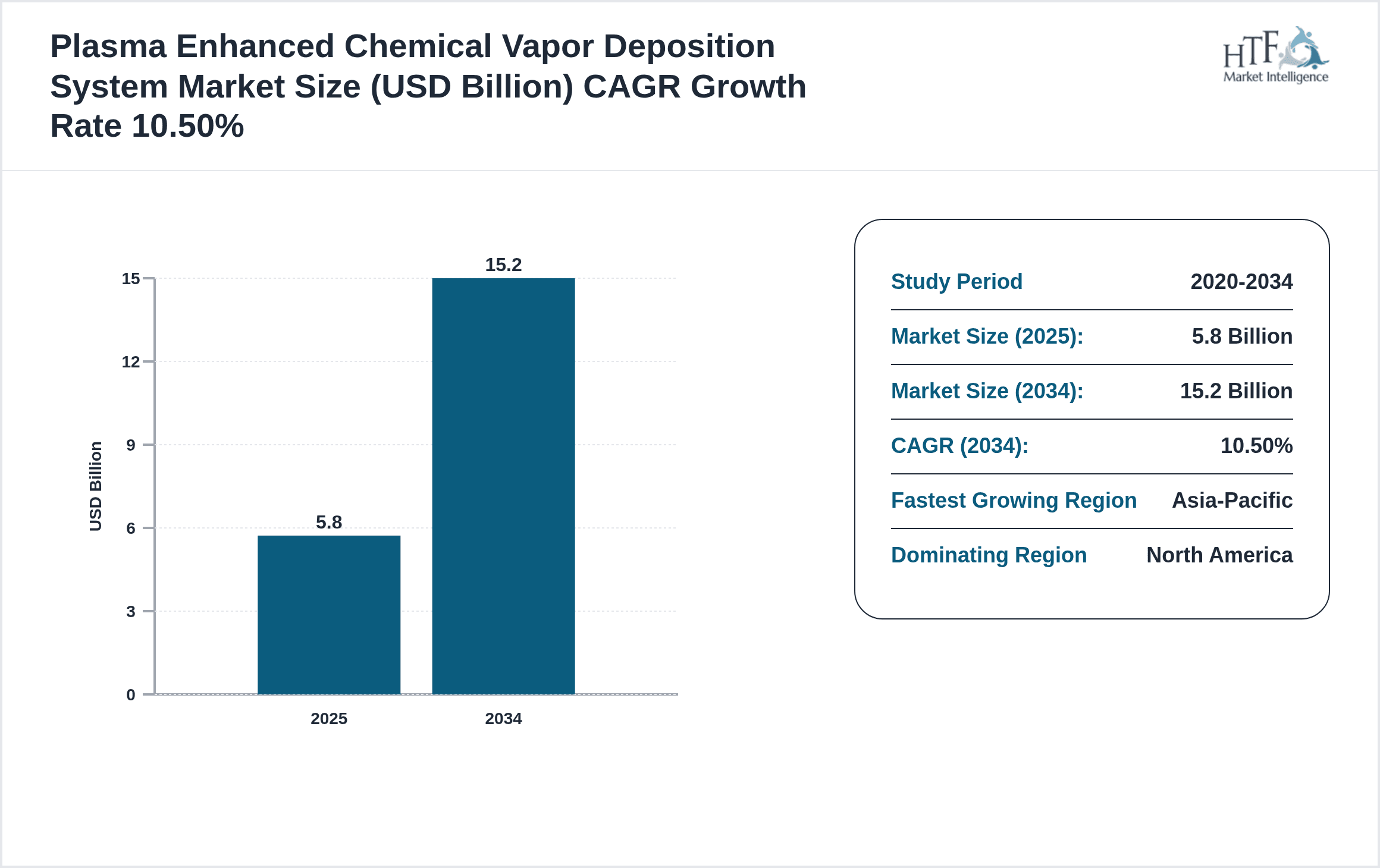
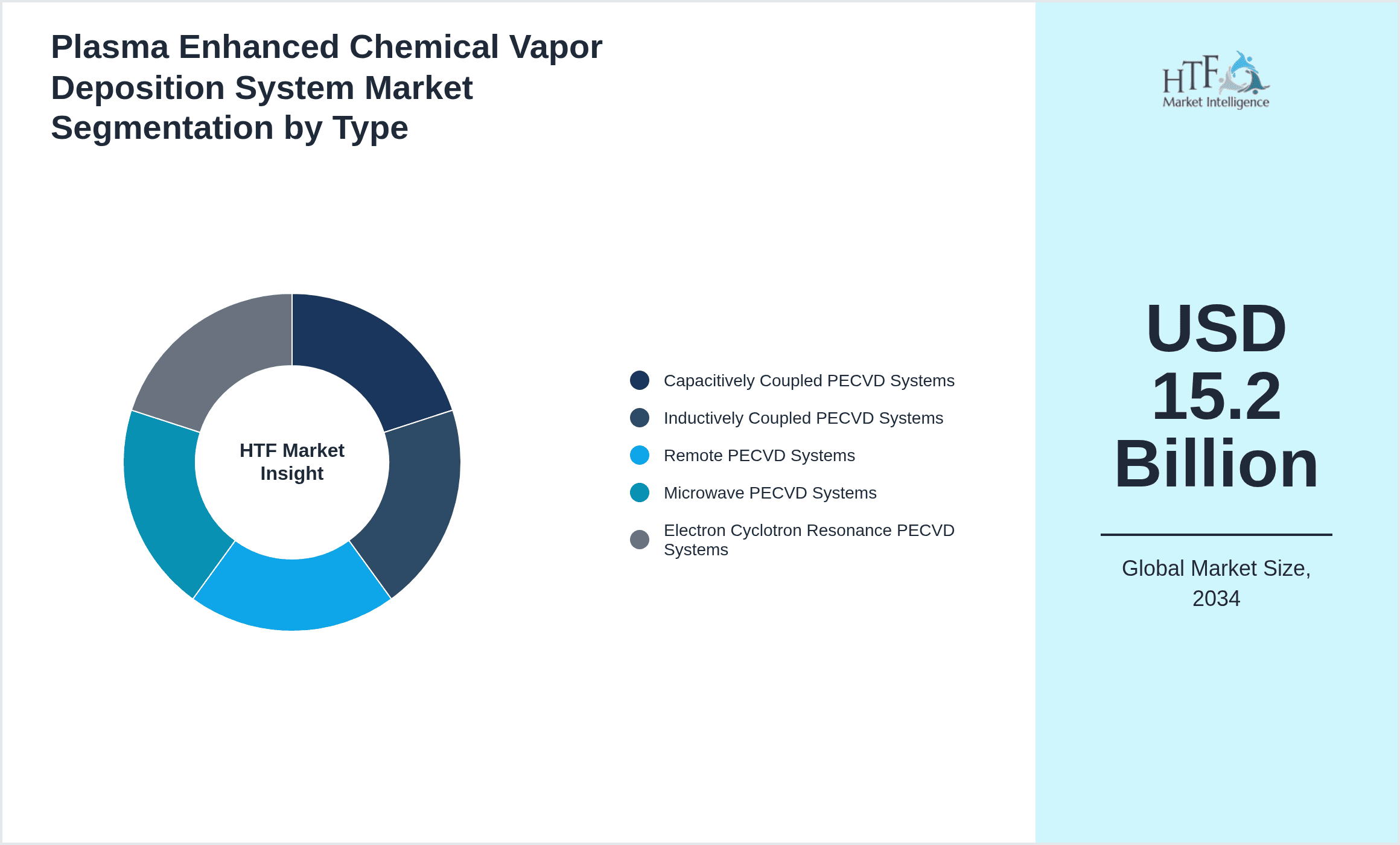
- •Key highlights include a base market valuation of USD 5.8 Billion in 2024 with a forecast to reach USD 15.2 Billion by 2034, driven by a CAGR of 10.5%. The market is predominantly led by North America, holding 34% market share, while Asia-Pacific exhibits the fastest growth at 14.3% CAGR. Inductively Coupled PECVD systems dominate the type segment, closely followed by Capacitively Coupled PECVD. Semiconductor manufacturing remains the leading application, with solar cell production as the secondary segment.
- •Strategically, the PECVD system market is critical to advancing electronics miniaturization and renewable energy solutions, offering stakeholders opportunities for innovation, regional expansion, and technological integration. Industry participants benefit from evolving process technologies and increasing demand across emerging economies.
Competitive Landscape
The competitive environment in the Global Plasma Enhanced Chemical Vapor Deposition System market is characterized by intense rivalry among established multinational corporations and innovative technology providers. Market players focus on continuous product innovation, enhancing system efficiency, and expanding global manufacturing footprints to secure market leadership. Strategic partnerships, technological advancements, and investments in R&D are common to differentiate offerings and improve process capabilities. Pricing strategies are balanced against quality and technology superiority to maintain competitive advantage. Furthermore, regional players in Asia-Pacific are rapidly increasing their market presence, intensifying competition. Barriers to entry include high capital requirements and stringent quality standards, positioning incumbent firms advantageously. The dynamic nature of semiconductor and renewable energy sectors further drives the competitive landscape, encouraging collaborations and mergers to consolidate market share and accelerate technology adoption globally.
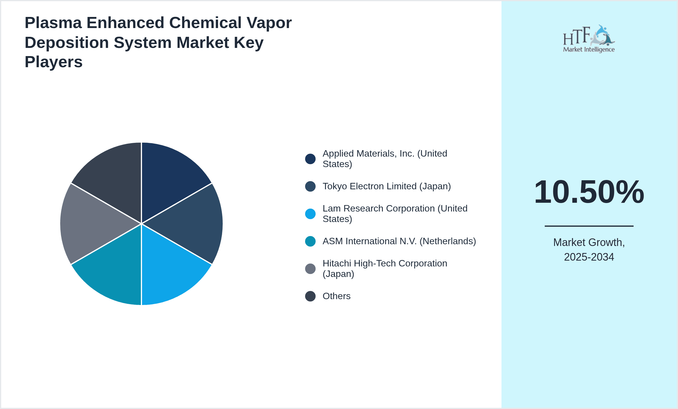
Leading Companies in Plasma Enhanced Chemical Vapor Deposition System Market
- •Applied Materials, Inc. (United States)
- •Tokyo Electron Limited (Japan)
- •Lam Research Corporation (United States)
- •ASM International N.V. (Netherlands)
- •Hitachi High-Tech Corporation (Japan)
- •Oxford Instruments PLC (United Kingdom)
- •ULVAC, Inc. (Japan)
- •Kokusai Electric Corporation (Japan)
- •Veeco Instruments Inc. (United States)
- •NexX Systems, Inc. (United States)
- •SENTECH Instruments GmbH (Germany)
- •Plasma-Therm LLC (United States)
- •PVA TePla AG (Germany)
- •Ferrotec Holdings Corporation (Japan)
- •MKS Instruments, Inc. (United States)
- •Diener Electronic GmbH + Co. KG (Germany)
- •CVD Equipment Corporation (United States)
- •Advanced Energy Industries, Inc. (United States)
- •Plasmatherm GmbH (Germany)
- •SPTS Technologies Limited (United Kingdom)
- •Veeco Instruments Inc. (United States)
- •Oxford Instruments Plasma Technology (United Kingdom)
- •Tystar Corporation (United States)
- •Plasma Process Group (United States)
- •Nissin Electric Co., Ltd. (Japan)

Market Breakdown
- •By Type
- ◦Capacitively Coupled PECVD Systems
- ◦Inductively Coupled PECVD Systems
- ◦Remote PECVD Systems
- ◦Microwave PECVD Systems
- ◦Electron Cyclotron Resonance PECVD Systems
- •By Application
- ◦Semiconductor Manufacturing
- ◦Solar Cell Production
- ◦Optical Coating
- ◦MEMS Fabrication
- ◦Other Industrial Applications
- •By End User
- ◦Electronics Manufacturers
- ◦Renewable Energy Companies
- ◦Optical Device Producers
- ◦Research & Development Institutes
- •By Distribution Channel
- ◦Direct Sales
- ◦Distributors and Resellers
- ◦Online Platforms
Growth Drivers
Expansion in semiconductor manufacturing due to rising demand for miniaturized electronic devices fuels the need for advanced PECVD systems, which offer precise thin film deposition critical for integrated circuits and memory devices. The growth of renewable energy sectors, particularly solar photovoltaics, also propels PECVD adoption as it enables efficient silicon nitride and oxide layer deposition essential for solar cell performance. Technological advancements in PECVD equipment, such as enhanced plasma sources and process controls, increase system throughput and film quality, attracting manufacturers. Additionally, increasing investments in R&D and capacity expansion by key players facilitate market growth. The growing electronics and solar markets in Asia-Pacific further stimulate demand, supported by government incentives for clean energy and electronics manufacturing hubs. Overall, the need for high-performance, cost-effective thin film solutions across multiple industries acts as a primary growth catalyst for the global Plasma Enhanced Chemical Vapor Deposition System market.
Market Trends
The market is witnessing a strong trend toward development of remote PECVD systems that minimize substrate damage and enable uniform coatings on complex geometries, essential for advanced semiconductor nodes. Integration of AI and machine learning into PECVD process controls is enhancing process repeatability and reducing downtime. Sustainable manufacturing practices are influencing equipment design, with energy-efficient plasma sources gaining traction. Collaborative innovation between equipment suppliers and semiconductor foundries is accelerating tailored system development to meet specific application requirements. Furthermore, the rise of flexible electronics and wearable devices is driving demand for PECVD systems capable of low-temperature processing on polymer substrates. Geographic expansion into emerging markets with growing electronics and solar manufacturing bases, especially in Asia-Pacific, is also shaping market dynamics and competitive strategies.
Market Restraints
High capital expenditure and operational costs associated with advanced Plasma Enhanced Chemical Vapor Deposition Systems pose significant barriers for small and medium enterprises, limiting market penetration. Complexity in process optimization and the need for skilled operators further constrain adoption in emerging economies. Additionally, stringent environmental regulations on plasma gas emissions and energy consumption increase compliance costs. Equipment downtime due to maintenance requirements and sensitivity to contamination impacts productivity, deterring some potential users. Competitive alternative thin-film deposition techniques, such as atomic layer deposition and sputtering, provide technological challenges by offering specific advantages in certain applications. These factors collectively restrain rapid market expansion and necessitate continuous innovation to reduce costs and improve operational efficiency.
Market Opportunities
Emerging applications in flexible and wearable electronics present significant opportunities for PECVD systems capable of low-temperature, uniform film deposition on flexible substrates. The growing adoption of advanced packaging technologies in semiconductors, such as 3D ICs, requires specialized PECVD solutions, opening new market segments. Expansion in solar photovoltaic installations globally, especially in Asia-Pacific and Latin America, drives demand for PECVD systems optimized for high-throughput solar cell production. Integration of AI-driven process monitoring offers potential for improved yield and reduced operational costs, appealing to high-volume manufacturers. Furthermore, strategic collaborations and joint ventures between equipment manufacturers and end-users can accelerate product innovation and market penetration. Upgrading legacy PECVD systems in established semiconductor hubs provides a lucrative replacement market. These opportunities combined position the global PECVD system market for sustained growth.
Market Challenges
The Plasma Enhanced Chemical Vapor Deposition System market faces challenges including managing the balance between equipment cost and performance to meet diverse customer needs. Rapid technological evolution necessitates continuous R&D investment, leading to high operational expenses. Supply chain disruptions impact availability of critical components, delaying production and delivery schedules. Variability in global regulatory frameworks complicates compliance and market entry strategies, especially concerning environmental and safety standards. Intense competition from established players and emerging regional manufacturers pressures pricing and margin sustainability. Additionally, scarcity of skilled workforce proficient in PECVD technologies limits operational efficiency and customer support. Addressing process uniformity and reproducibility across different substrate materials remains a technical challenge, impacting product quality and customer satisfaction.
Regulatory Framework
Recent regulatory updates from 2023 to 2024 emphasize stricter environmental compliance related to plasma gas emissions and energy efficiency for PECVD equipment manufacturers globally. Regions such as North America and Europe have introduced enhanced guidelines mandating reduced greenhouse gas emissions and adoption of eco-friendly plasma sources. Safety standards for operator exposure to plasma and toxic gases have been fortified, requiring improved containment and monitoring systems within PECVD units. Additionally, regulations incentivizing energy-efficient manufacturing practices encourage equipment innovation towards reduced power consumption. Compliance with these evolving standards impacts design and operational protocols, influencing cost structures and market accessibility. Manufacturers are increasingly aligning product development with these regulatory frameworks to ensure global market compatibility and foster sustainable growth in the Plasma Enhanced Chemical Vapor Deposition System market.
Industry Insights
In March 2023, Applied Materials, Inc. launched an advanced inductively coupled PECVD system featuring enhanced plasma uniformity and throughput, targeting next-generation semiconductor nodes. This innovation supports manufacturers aiming for higher yield and lower defect rates in complex chip architectures. In September 2024, Tokyo Electron Limited introduced a remote PECVD system optimized for flexible electronics production, addressing growing demand in wearable technology markets. These developments underscore the industry's focus on improving process precision and expanding application scopes to meet evolving customer requirements worldwide.
Mergers & Acquisitions
- •In July 2023, Lam Research Corporation completed the acquisition of a specialist PECVD equipment manufacturer, enhancing its product portfolio with innovative remote plasma technologies. This strategic move strengthens Lam Research's market position in advanced semiconductor equipment by integrating complementary technologies and expanding its customer base globally. The acquisition supports accelerated R&D efforts and broadens application coverage, particularly in next-generation memory and logic devices.
- •In November 2024, ASM International N.V. acquired a niche provider of microwave PECVD systems focused on solar cell manufacturing. This acquisition aims to leverage ASM's global reach and technological expertise to scale production capabilities and accelerate adoption of energy-efficient PECVD solutions in the renewable energy sector. It also facilitates cross-technology integration to enhance system performance and operational efficiency.
Recent Industry News
- •On 15th January 2024, Oxford Instruments Plasma Technology announced a partnership with a leading semiconductor foundry to co-develop PECVD systems tailored for 3D integrated circuits. This collaboration aims to optimize deposition uniformity and throughput to meet stringent manufacturing specifications, driving innovation in high-density chip packaging. Source: Official Company Website
- •On 3rd May 2023, Veeco Instruments Inc. expanded its manufacturing facility in the United States to increase production capacity of inductively coupled PECVD systems, responding to rising demand in solar cell and semiconductor markets. The expansion includes advanced automation to improve quality and reduce lead times. Source: Industry Publication
- •On 22nd August 2024, ULVAC, Inc. launched a new electron cyclotron resonance PECVD system that offers ultra-low damage film deposition for sensitive MEMS applications. The system incorporates real-time process monitoring to enhance reproducibility and yield, supporting next-generation device fabrication. Source: Official Press Release
- •On 10th November 2022, Hitachi High-Tech Corporation announced a strategic alliance with a major solar panel manufacturer to develop high-throughput PECVD equipment optimized for large-scale photovoltaic production, aiming to improve film quality and reduce energy consumption. Source: Industry News Outlet
Market Statistics
- •CAGR by 2034: 10.5%
- •Market Size by 2034: USD 15.2 Billion
- •Market Size in 2025: USD 6.4 Billion
- •Dominating Type: Inductively Coupled PECVD
- •Next-Following Type: Capacitively Coupled PECVD
- •Dominating Application: Semiconductor Manufacturing
- •Next-Following Application: Solar Cell Production
- •Dominating Region: North America
- •Second-Leading Region: Europe
- •Region with Highest Growth Rate: Asia-Pacific
- •Dominating Country: United States
Market Share Table
- •Market Share (%) of Dominating vs Followed Type: Inductively Coupled PECVD 40%, Capacitively Coupled PECVD 28%
- •Market Share (%) of Dominating vs Followed Application: Semiconductor Manufacturing 45%, Solar Cell Production 25%
- •Growth Rate (%) of Dominating vs Followed Type: Inductively Coupled PECVD 11.2%, Capacitively Coupled PECVD 8.7%
- •Growth Rate (%) of Dominating vs Followed Application: Semiconductor Manufacturing 12.0%, Solar Cell Production 9.4%
Top Companies Profiled in Plasma Enhanced Chemical Vapor Deposition System Market
- •Applied Materials, Inc. (United States)
- •Tokyo Electron Limited (Japan)
- •Lam Research Corporation (United States)
- •ASM International N.V. (Netherlands)
- •Hitachi High-Tech Corporation (Japan)
Regional Outlook
The North America currently holds a significant share of the market, primarily due to several key factors: increasing consumption rates, a burgeoning population, and robust economic momentum. These elements collectively drive demand, positioning this region as a leader in the market. On the other hand, Asia-Pacific is rapidly emerging as the fastest-growing area within the industry. This remarkable growth can be attributed to swift infrastructure development, the expansion of various industrial sectors, and a marked increase in consumer demand. These dynamics make this region a crucial player in shaping future market growth.
In our report, we cover a comprehensive analysis of the following regions and countries:
- North America
- LATAM
- West Europe
- Central & Eastern Europe
- Northern Europe
- Southern Europe
- East Asia
- Southeast Asia
- South Asia
- Central Asia
- Oceania
- MEA
| Feature | Details |
|---|---|
| Base Year Market Size | USD 5.8 Billion |
| Forecast Year Market Size | USD 15.2 Billion |
| CAGR | 10.5% |
| Forecast Period | 2026 to 2033 |
| YoY Growth | 10% |
| Scope of Report | Market is segmented by Type (Capacitively Coupled PECVD Systems, Inductively Coupled PECVD Systems, Remote PECVD Systems, Microwave PECVD Systems, Electron Cyclotron Resonance PECVD Systems), Application (Semiconductor Manufacturing, Solar Cell Production, Optical Coating, MEMS Fabrication, Other Industrial Applications), End User (Electronics Manufacturers, Renewable Energy Companies, Optical Device Producers, Research & Development Institutes), Distribution Channel (Direct Sales, Distributors and Resellers, Online Platforms) |
| Regions Covered | North America, LATAM, West Europe, Central & Eastern Europe, Northern Europe, Southern Europe, East Asia, Southeast Asia, South Asia, Central Asia, Oceania, MEA |
| Key Companies | Applied Materials, Inc. (United States), Tokyo Electron Limited (Japan), Lam Research Corporation (United States), ASM International N.V. (Netherlands), Hitachi High-Tech Corporation (Japan), Oxford Instruments PLC (United Kingdom), ULVAC, Inc. (Japan), Kokusai Electric Corporation (Japan), Veeco Instruments Inc. (United States), NexX Systems, Inc. (United States), SENTECH Instruments GmbH (Germany), Plasma-Therm LLC (United States), PVA TePla AG (Germany), Ferrotec Holdings Corporation (Japan), MKS Instruments, Inc. (United States), Diener Electronic GmbH + Co. KG (Germany), CVD Equipment Corporation (United States), Advanced Energy Industries, Inc. (United States), Plasmatherm GmbH (Germany), SPTS Technologies Limited (United Kingdom), Veeco Instruments Inc. (United States), Oxford Instruments Plasma Technology (United Kingdom), Tystar Corporation (United States), Plasma Process Group (United States), Nissin Electric Co., Ltd. (Japan) |
Global Plasma Enhanced Chemical Vapor Deposition System Market Size, Growth & Revenue 2024-2034 - Table of Contents
Frequently Asked Questions (FAQ):
The Compact Track Loaders market is expected to see value worth 5.3 Billion in 2025.
North America currently leads the market with approximately 45% market share, followed by Europe at 28% and Asia-Pacific at 22%. The remaining regions account for 5% of the global market.
Key growth drivers include increasing construction activities, rising demand for versatile equipment in agriculture, technological advancements in track loader design, and growing preference for compact equipment in urban construction projects.