
Japan Tungsten CMP Slurries for Metal Removal Market Size, Growth & Revenue 2024-2034
Japan Tungsten CMP Slurries for Metal Removal Market is segmented by Type (Oxide-based Slurries, Abrasive-based Slurries, Chemical-based Slurries, Hybrid Slurries, Specialty Slurries), Application (Semiconductor Fabrication, Data Storage Devices, MEMS (Micro-Electro-Mechanical Systems), Flat Panel Displays, Others), End User (Semiconductor Manufacturers, Display Manufacturers, Data Storage Companies, MEMS Producers), Distribution Channel (Direct Sales, Distributors, Online Platforms), and Geography (Hokkaido, Tohoku, Kanto, Chubu, Kansai, Chugoku, Shikoku, Kyushu)
Pricing
Report Overview
Executive Summary
- •The Japan Tungsten CMP Slurries for Metal Removal Market comprises specialized chemical mechanical planarization slurries developed for tungsten layer removal in semiconductor and electronic device production, emphasizing precision, quality, and process efficiency within Japan's advanced manufacturing landscape.
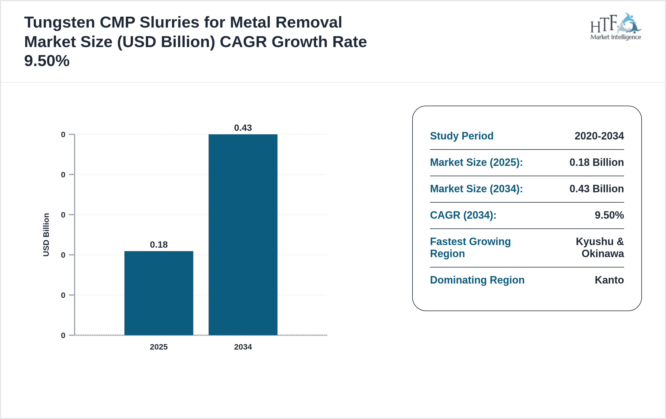
- •Key market highlights include a projected CAGR of 9.5% from 2024 to 2034, driven by semiconductor fabrication growth, increasing demand for high-performance electronics, and technological advancements in slurry formulations tailored to tungsten CMP processes.
- •This market offers strategic value to semiconductor manufacturers, slurry producers, and technology innovators by enabling defect-free wafer planarization, supporting Japan's position as a global semiconductor hub, and fostering sustainable production practices aligned with regulatory frameworks.
Competitive Landscape
The Japan Tungsten CMP Slurries for Metal Removal Market exhibits intense competition characterized by both global chemical suppliers and specialized local manufacturers striving for technological leadership. Companies invest heavily in R&D to innovate slurry chemistries that enhance removal rates, selectivity, and surface quality while minimizing defects. Strategic partnerships with semiconductor fabs, emphasis on sustainable formulations, and maintaining supply chain reliability are critical competitive factors. The rivalry fosters continuous product differentiation, adoption of automation in slurry delivery, and expansion into emerging semiconductor segments. Market entry barriers include high technical expertise, strict quality control, and compliance with Japan's regulatory environment. Competitive strategies focus on innovation, customization, and collaboration with end-users to sustain market share and respond swiftly to evolving semiconductor process requirements.
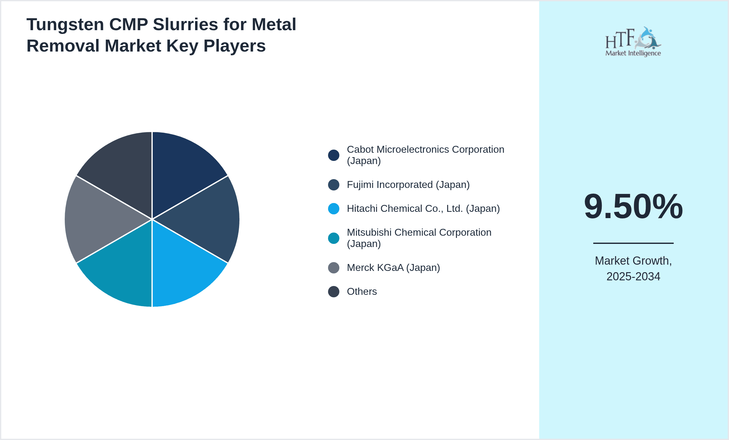
Leading Companies in Japan Tungsten CMP Slurries for Metal Removal Market
- •Cabot Microelectronics Corporation (Japan)
- •Fujimi Incorporated (Japan)
- •Hitachi Chemical Co., Ltd. (Japan)
- •Mitsubishi Chemical Corporation (Japan)
- •Merck KGaA (Japan)
- •DuPont de Nemours, Inc. (Japan)
- •Solvay S.A. (Japan)
- •JSR Corporation (Japan)
- •Tosoh Corporation (Japan)
- •Ferro Corporation (Japan)
- •Sumitomo Chemical Co., Ltd. (Japan)
- •Nippon Paint Holdings Co., Ltd. (Japan)
- •Asahi Glass Co., Ltd. (Japan)
- •Sekisui Chemical Co., Ltd. (Japan)
- •Nissan Chemical Corporation (Japan)
- •Shin-Etsu Chemical Co., Ltd. (Japan)
- •Tokuyama Corporation (Japan)
- •MGC Chemicals Corporation (Japan)
- •Sumitomo Electric Industries, Ltd. (Japan)
- •3M Company (Japan)
- •BASF Japan Ltd. (Japan)
- •Showa Denko K.K. (Japan)
- •Toray Industries, Inc. (Japan)
- •Nitto Denko Corporation (Japan)
- •Hitachi High-Technologies Corporation (Japan)

Market Breakdown
- •By Type
- ◦Oxide-based Slurries
- ◦Abrasive-based Slurries
- ◦Chemical-based Slurries
- ◦Hybrid Slurries
- ◦Specialty Slurries
- •By Application
- ◦Semiconductor Fabrication
- ◦Data Storage Devices
- ◦MEMS (Micro-Electro-Mechanical Systems)
- ◦Flat Panel Displays
- ◦Others
- •By End User
- ◦Semiconductor Manufacturers
- ◦Display Manufacturers
- ◦Data Storage Companies
- ◦MEMS Producers
- •By Distribution Channel
- ◦Direct Sales
- ◦Distributors
- ◦Online Platforms
Growth Drivers
- •Rising demand for advanced semiconductor devices in Japan, driven by the proliferation of IoT, 5G, and AI technologies, is significantly increasing the need for high-quality tungsten CMP slurries to enable precise metal removal and device miniaturization.
- •Continuous technological advancements in slurry formulations, including hybrid and specialty slurries, enhance removal efficiency and selectivity, which boosts adoption among semiconductor fabs seeking process optimization and defect reduction.
- •Government initiatives supporting semiconductor manufacturing expansion and innovation in Japan are fueling investments in CMP slurry production technologies, fostering market growth through subsidies and research collaborations.
- •Increasing integration of tungsten in semiconductor interconnects due to its superior conductivity and thermal properties is driving demand for specialized CMP slurries tailored to tungsten metal removal.
- •Growing focus on sustainable manufacturing practices encourages the development of eco-friendly CMP slurries, attracting environmentally conscious semiconductor manufacturers and expanding market opportunities.

Market Trends
- •Adoption of hybrid CMP slurries combining chemical and abrasive properties is gaining traction in Japan, offering enhanced planarization rates and reduced defectivity, aligning with the industry's push toward next-generation semiconductor nodes.
- •Increasing automation and precision in slurry delivery systems are improving CMP process control and consistency across Japanese fabs, supporting higher yield rates and lower operational costs.
- •Collaborations between slurry manufacturers and semiconductor companies in Japan are fostering co-development initiatives to tailor slurry chemistries for specific wafer architectures and process steps.
- •Rising emphasis on CMP slurry recyclability and waste treatment solutions reflects Japan’s commitment to environmental sustainability and regulatory compliance within the semiconductor manufacturing ecosystem.
- •Expansion of CMP slurry applications beyond semiconductors into MEMS and flat panel display industries is diversifying the market and enabling technology cross-pollination.
Market Opportunities
- •Expanding semiconductor foundry capacities in Japan present significant opportunities for CMP slurry suppliers to establish long-term supply contracts and customize products for evolving process technologies.
- •Development of low-abrasion and high-selectivity slurries tailored for emerging 3D semiconductor architectures can unlock new application segments and premium pricing models.
- •Collaborative R&D partnerships with academic institutions and government labs could accelerate innovation in slurry chemistry, driving competitive advantage and market penetration.
- •Growing demand for environmentally friendly and biodegradable CMP slurries provides avenues for product differentiation and compliance with tightening Japanese environmental regulations.
- •Increasing use of CMP slurries in non-semiconductor sectors such as data storage and MEMS offers diversification potential and revenue growth beyond traditional markets.
Market Challenges
- •Stringent quality and purity requirements in tungsten CMP processes pose technical challenges for slurry manufacturers, necessitating high precision in formulation and process consistency.
- •High development and production costs for advanced CMP slurries limit entry opportunities for smaller players and increase pressure on profit margins across the industry.
- •Supply chain disruptions and raw material price volatility can impact slurry availability and cost stability, affecting semiconductor fabs’ production schedules in Japan.
- •Regulatory compliance related to chemical safety and environmental impact requires continuous monitoring and adaptation by slurry producers, increasing operational complexity.
- •Competitive pressure from global slurry suppliers with larger scale and R&D budgets challenges Japan-based companies to maintain technological leadership and market share.
Regulatory Overview
- •Between 2020 and 2024, Japan implemented updated chemical management laws focusing on reducing hazardous substance usage in manufacturing, impacting CMP slurry formulations to enhance environmental safety.
- •The Ministry of Economy, Trade and Industry (METI) has introduced guidelines for semiconductor manufacturing waste disposal, compelling slurry manufacturers to adopt eco-friendly product designs and waste treatment methods.
- •Regulations on workplace chemical exposure limits have been tightened, necessitating improved handling protocols and safety measures for CMP slurry production facilities in Japan.
- •Japan’s inclusion in international chemical safety agreements promotes harmonization of slurry product standards, facilitating exports and cross-border technology transfer.
- •Government incentives for green technology adoption encourage slurry producers to innovate sustainable solutions, aligning regulatory compliance with market demand for environmentally responsible products.
Industry Insights
- •In March 2024, Fujimi Incorporated launched a new hybrid tungsten CMP slurry designed to significantly enhance removal rates while reducing wafer surface defects, targeting next-generation semiconductor fabrication processes in Japan. This innovation underscores the company’s commitment to addressing evolving industry needs and supporting Japan’s semiconductor ecosystem expansion.
- •Hitachi Chemical Co., Ltd. announced in November 2023 a strategic partnership with a leading Japanese semiconductor foundry to co-develop customized CMP slurry solutions, aiming to improve planarization efficiency and process integration. This collaboration highlights the growing trend of supplier-end user cooperation within Japan’s CMP slurry market.
Mergers & Acquisitions
- •In August 2024, Mitsubishi Chemical Corporation completed the acquisition of a specialized CMP slurry startup based in the Kansai region, enhancing its product portfolio with advanced tungsten slurry technologies. This strategic move strengthens Mitsubishi’s position in Japan’s CMP market, enabling it to offer comprehensive solutions tailored to semiconductor manufacturers’ evolving demands.
- •In February 2023, JSR Corporation acquired a minority stake in a chemical abrasives firm located in Tohoku, aiming to integrate innovative abrasive materials into its tungsten CMP slurry formulations. This investment reflects the company's strategy to enhance R&D capabilities and accelerate product development in Japan’s competitive CMP slurry landscape.
Recent Industry News
- •15th January 2025, Cabot Microelectronics Corporation announced the launch of an eco-friendly tungsten CMP slurry variant in Japan, emphasizing reduced chemical waste and higher process stability. The product is designed to meet stringent environmental regulations and support sustainable semiconductor manufacturing, reinforcing Cabot’s leadership in the Japanese market. Source: Company press release
- •10th March 2025, Sumitomo Chemical Co., Ltd. expanded its CMP slurry production facility in the Chubu region to meet increasing demand from semiconductor fabs adopting advanced tungsten planarization techniques. The expansion includes state-of-the-art process control technologies aimed at enhancing slurry quality and supply reliability. Source: Industry publication
- •22nd May 2025, Merck KGaA entered into a collaborative agreement with a major Japanese semiconductor equipment manufacturer to co-develop next-generation CMP slurry formulations targeting ultra-fine tungsten features, aiming to improve device performance and yield. Source: Official company announcement
- •30th July 2025, DuPont de Nemours, Inc. introduced a novel chemical-based tungsten CMP slurry in Japan featuring enhanced selectivity and defect mitigation capabilities, addressing the growing complexity of semiconductor process nodes. This launch aligns with industry trends toward higher precision and reduced contamination. Source: Industry news portal
Market Statistics
- •CAGR by 2034: 9.5%
- •Market Size by 2034: USD 430 Million
- •Market Size in 2025: USD 195 Million
- •Dominating Type: Oxide-based Slurries; Next-following Type: Hybrid Slurries
- •Dominating Application: Semiconductor Fabrication; Next-following Application: Data Storage Devices
- •Dominating Region: Kanto; Second-leading Region: Kansai
- •Region with Highest Growth Rate: Kyushu & Okinawa
- •Dominating Country: Japan
Market Share Table
- •Market Share (%) of Dominating vs Followed Type: Oxide-based Slurries 45%, Hybrid Slurries 25%
- •Market Share (%) of Dominating vs Followed Application: Semiconductor Fabrication 55%, Data Storage Devices 20%
- •Growth Rate (%) of Dominating vs Followed Type: Oxide-based Slurries 8.7%, Hybrid Slurries 12.3%
- •Growth Rate (%) of Dominating vs Followed Application: Semiconductor Fabrication 9.0%, Data Storage Devices 8.0%
Top Companies Profiled in Japan Tungsten CMP Slurries for Metal Removal Market
- •Cabot Microelectronics Corporation (Japan)
- •Fujimi Incorporated (Japan)
- •Hitachi Chemical Co., Ltd. (Japan)
- •Mitsubishi Chemical Corporation (Japan)
- •Merck KGaA (Japan)
Regional Outlook
The Kanto currently holds a significant share of the market, primarily due to several key factors: increasing consumption rates, a burgeoning population, and robust economic momentum. These elements collectively drive demand, positioning this region as a leader in the market. On the other hand, Kyushu & Okinawa is rapidly emerging as the fastest-growing area within the industry. This remarkable growth can be attributed to swift infrastructure development, the expansion of various industrial sectors, and a marked increase in consumer demand. These dynamics make this region a crucial player in shaping future market growth.
In our report, we cover a comprehensive analysis of the following regions and countries:
- Hokkaido
- Tohoku
- Kanto
- Chubu
- Kansai
- Chugoku
- Shikoku
- Kyushu
| Feature | Details |
|---|---|
| Base Year Market Size | USD 180 Million |
| Forecast Year Market Size | USD 430 Million |
| CAGR | 9.5% |
| Forecast Period | 2026 to 2033 |
| YoY Growth | 9.1% |
| Scope of Report | Market is segmented by Type (Oxide-based Slurries, Abrasive-based Slurries, Chemical-based Slurries, Hybrid Slurries, Specialty Slurries), Application (Semiconductor Fabrication, Data Storage Devices, MEMS (Micro-Electro-Mechanical Systems), Flat Panel Displays, Others), End User (Semiconductor Manufacturers, Display Manufacturers, Data Storage Companies, MEMS Producers), Distribution Channel (Direct Sales, Distributors, Online Platforms) |
| Regions Covered | Hokkaido, Tohoku, Kanto, Chubu, Kansai, Chugoku, Shikoku, Kyushu |
| Key Companies | Cabot Microelectronics Corporation (Japan), Fujimi Incorporated (Japan), Hitachi Chemical Co., Ltd. (Japan), Mitsubishi Chemical Corporation (Japan), Merck KGaA (Japan), DuPont de Nemours, Inc. (Japan), Solvay S.A. (Japan), JSR Corporation (Japan), Tosoh Corporation (Japan), Ferro Corporation (Japan), Sumitomo Chemical Co., Ltd. (Japan), Nippon Paint Holdings Co., Ltd. (Japan), Asahi Glass Co., Ltd. (Japan), Sekisui Chemical Co., Ltd. (Japan), Nissan Chemical Corporation (Japan), Shin-Etsu Chemical Co., Ltd. (Japan), Tokuyama Corporation (Japan), MGC Chemicals Corporation (Japan), Sumitomo Electric Industries, Ltd. (Japan), 3M Company (Japan), BASF Japan Ltd. (Japan), Showa Denko K.K. (Japan), Toray Industries, Inc. (Japan), Nitto Denko Corporation (Japan), Hitachi High-Technologies Corporation (Japan) |
Japan Tungsten CMP Slurries for Metal Removal Market Size, Growth & Revenue 2024-2034 - Table of Contents
Frequently Asked Questions (FAQ):
The Compact Track Loaders market is expected to see value worth 5.3 Billion in 2025.
North America currently leads the market with approximately 45% market share, followed by Europe at 28% and Asia-Pacific at 22%. The remaining regions account for 5% of the global market.
Key growth drivers include increasing construction activities, rising demand for versatile equipment in agriculture, technological advancements in track loader design, and growing preference for compact equipment in urban construction projects.