
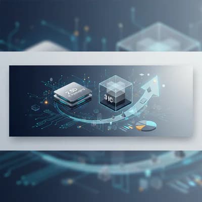
Unlocking Innovation with 3D IC and 2.5D IC Packaging Technologies
Explore how 3D IC and 2.5D IC packaging revolutionize semiconductor technology with enhanced performance, space efficiency, and industry applications.
Introduction
In the rapidly evolving semiconductor industry, 3D IC and 2.5D IC packaging have emerged as pivotal technologies that redefine how integrated circuits (ICs) are designed and manufactured. These advanced packaging techniques address the increasing demand for higher performance, reduced power consumption, and miniaturized form factors in modern electronics.
Understanding the nuances of 3D and 2.5D IC packaging is essential for businesses aiming to stay competitive in markets such as mobile devices, high-performance computing, and automotive electronics. This article delves into the core concepts, industry applications, market trends, advantages, challenges, and future outlook of these cutting-edge packaging solutions.
Technology Overview: What Are 3D IC and 2.5D IC Packaging?
3D IC packaging refers to the vertical stacking of multiple integrated circuit dies within a single package, interconnected through technologies like through-silicon vias (TSVs). This vertical integration enables higher density and performance by shortening interconnect distances and enabling heterogeneous integration of various semiconductor technologies.
On the other hand, 2.5D IC packaging involves placing multiple dies side-by-side on an interposer—a silicon or organic substrate—that provides high-density interconnections between the chips. Unlike 3D ICs, 2.5D packages do not stack dies vertically but leverage the interposer to achieve high bandwidth and power efficiency.
Key technologies involved include TSVs, microbumps, interposers, and advanced substrate materials. These enable improved electrical performance and thermal management compared to traditional package designs.
Industry Applications & Use Cases
The adoption of 3D IC and 2.5D IC packaging spans several high-growth sectors. For instance, in mobile devices, these packaging methods enable increasingly powerful System-on-Chip (SoC) configurations that support AI and 5G functionality while maintaining a slim profile.
In the realm of high-performance computing (HPC), companies like AMD and NVIDIA utilize 2.5D packaging with silicon interposers to integrate multiple GPU dies, resulting in significant improvements in compute throughput and energy efficiency. A notable example is AMD’s Radeon Vega GPUs, which leverage 2.5D packaging to deliver superior graphics performance.
The automotive sector benefits from 3D IC packaging as well, especially in advanced driver-assistance systems (ADAS) and autonomous vehicles, where space constraints and high reliability standards demand compact yet robust IC solutions.
Furthermore, data centers increasingly rely on 3D stacking to improve memory bandwidth and processor interconnects, driving faster data processing and reduced latency.
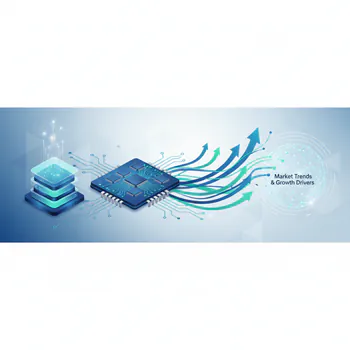
Market Trends & Growth Drivers
The global market for 3D IC and 2.5D IC packaging is witnessing robust growth, driven by the explosion of IoT devices and the push for enhanced AI capabilities. According to industry reports, the 3D IC packaging market alone is expected to grow at a CAGR of over 20% through 2028.
Key growth drivers include the need for improved power efficiency, miniaturization of electronic devices, and the integration of diverse semiconductor technologies such as logic, memory, and sensors within a single package.
Additionally, advancements in semiconductor fabrication, such as finer lithography nodes and improved TSV manufacturing processes, are accelerating adoption. Major semiconductor foundries and OSAT (Outsourced Semiconductor Assembly and Test) providers are investing heavily in 3D and 2.5D packaging capabilities to meet this demand.
Emerging markets like wearables, augmented reality (AR), and edge computing also fuel demand, necessitating compact, high-performance packaging solutions.
Market Trends & Growth Drivers
Benefits & Advantages
- Enhanced Performance: Shorter interconnect distances in 3D ICs and high-density interposers in 2.5D ICs significantly reduce signal delay and power consumption.
- Space Efficiency: Vertical stacking or side-by-side placement allows for miniaturized designs critical in mobile and wearable applications.
- Heterogeneous Integration: Facilitates combining chips built on different process nodes or materials, enabling multifunctional devices.
- Improved Thermal Management: Advanced packaging structures help dissipate heat more effectively, enhancing reliability.
- Competitive Edge & ROI: Businesses adopting these technologies gain faster time-to-market and higher product differentiation, translating into improved ROI.
Challenges & Future Outlook
Despite numerous advantages, 3D IC and 2.5D IC packaging face several challenges. The manufacturing complexity increases costs and reduces yields, especially with the precision required for TSV alignment and interposer fabrication.
Thermal management remains a hurdle due to the heat generated in densely packed chips. Innovations in materials and cooling solutions are ongoing to mitigate this.
Moreover, standardization across industry players is limited, which can impede interoperability and scalability.
Looking ahead, the future is promising. Research into wafer-to-wafer bonding, advanced interposers (including silicon photonics), and AI-driven design optimization is expected to overcome current limitations.
Industry analysts predict that by 2030, 3D and 2.5D packaging will be standard in most high-end semiconductor products, further driven by the rise of AI, 6G, and quantum computing technologies.
Conclusion
In summary, 3D IC and 2.5D IC packaging represent transformative steps in semiconductor design and manufacturing, offering substantial benefits in performance, miniaturization, and integration capabilities. As industries demand more powerful, energy-efficient, and compact devices, these packaging solutions become indispensable.
Businesses that invest in understanding and leveraging these advanced packaging techniques can unlock significant competitive advantages and prepare for the future of electronics innovation. By navigating current challenges and embracing emerging trends, the semiconductor industry is set to revolutionize how integrated circuits are constructed and deployed in the coming decade.
Need More Details on Market Players and Competitors?
Tagged in